Optical modulator

a technology of optical modulator and optical modulator, applied in the field of optical modulator, can solve the problems of increasing the number of optical modulators, high cost of ln optical modulators, and still encountering problems to be solved, so as to reduce the driving voltage, reduce the relative permittivity, and reduce the effect of microwave equivalent refractive index

Inactive Publication Date: 2012-06-19
ANRITSU CORP
View PDF10 Cites 0 Cited by
  • Summary
  • Abstract
  • Description
  • Claims
  • Application Information

AI Technical Summary

Benefits of technology

[0028]It is, therefore, an object of the present invention to provide an LN optical modulator to solve the problems in accordance with the examples of the prior art, which can have a wide optical modulation bandwidth, proper characteristic impedance, and low driving voltage, while reducing the cost and improving the process yield.
[0041]The optical modulator according to this invention is constructed such that the bottom surface between the ridge portions is formed not to be parallel to the top part of the ridge portion, but to be inclined so that the bottom surface has a downward convex to the z-cut LN substrate. This results in the fact that the optical modulator is constructed so that most of the electric lines of force generated from the high frequency electric signal between the center electrode and the ground electrode can effectively feel the air having low relative permittivity. To be more precise, most of the electric lines of force pass through the air, while the electric lines of force are appropriately distributed in the z-cut LN substrate and in the air. This makes it possible to efficiently reduce the microwave equivalent refractive index of the high frequency electric signal so that the difference between the microwave equivalent refractive index and the effective refractive index of the optical waveguide can be small, while enabling the characteristic impedance of the high frequency electric signal to be closer to 50Ω. In addition, this constitution makes it possible to distinctly confine the electric lines of force generated from the high frequency electric signal in the ridge portion, which results in reducing the driving voltage. Therefore, this invention can widen the optical modulation bandwidth, reduce impedance mismatch with outer driving circuit, and lower the driving voltage. In addition, the fact that the bottom surface between the ridge portions is inclined (preferably to have the center portion of the bottom surface deepest) is equivalent to the fact that the bottom surface is deep (i.e. the ridge portion is high) for the electric lines of force having downward convex shape. The height of the ridge portion should not be too high or too low, and there is an optimum height from the standpoint of the optical modulation efficiency. By applying this invention, the electric lines of force can regard the bottom surface between the ridge portions as being deeply formed. Therefore, the LN optical modulator can have an optimum construction from the viewpoint of optical modulation efficiency even with low ridge portions, which results in improving the modulation characteristics. Moreover, the LN optical modulator can reduce the manufacturing cost and improve the process yield due to the fact that the height of the ridge portions can be lowered. Furthermore, from the viewpoint of the optical modulation characteristics, it is preferable that the bottom surface between the ridge portions is formed along the electric lines of force having a curvature of downward convex. That is to say, the LN optical modulator can maximally utilize the modulation characteristics while improving the manufacturing process yield by forming the bottom surface with optimum inclination in response to construction parameters such as thickness and width of the traveling wave electrode, thickness of the buffer layer, width and height of the ridge portions, and gap between the center electrode and the ground electrode.

Problems solved by technology

The optical modulator according to the second prior art, however, still encounters a problem to be solved.
This results in increasing the number of processes to form the ridge portions, thereby resulting in high cost of LN optical modulator and low process yield.
However, the optical modulation characteristics are deteriorated in some degree, which results in the increase in the microwave equivalent refractive index nm and the reduction in the characteristics impedance, due to the fact that the electric lines of force 17 between the center electrode and the ground electrodes generated by the high frequency electric signal are passed through the z-cut LN substrate 1 beyond necessity resulting from the fact that the bottom surface between the ridge portions is parallel with the top part of the ridge portion.
This results in increasing the number of processes to form the ridge portions, thereby resulting in high cost of LN optical modulator.
However, it is difficult to form the ridge portion to have the optimum height by the process of dry etching with a gas in the form of plasma, due to the fact that the z-cut LN substrate is extremely hard.
Therefore, the advantages of the optical modulator with ridge structure have not been maximally developed.
Moreover, the depth where the z-cut LN substrate is etched tends to vary or the z-cut LN substrate may be cracked during the etching process, as the time length to form the ridge portion becomes longer.
This results in deteriorating the process yield of the LN optical modulator.

Method used


Image

  • Optical modulator
  • Optical modulator
  • Optical modulator

Examples


first embodiment

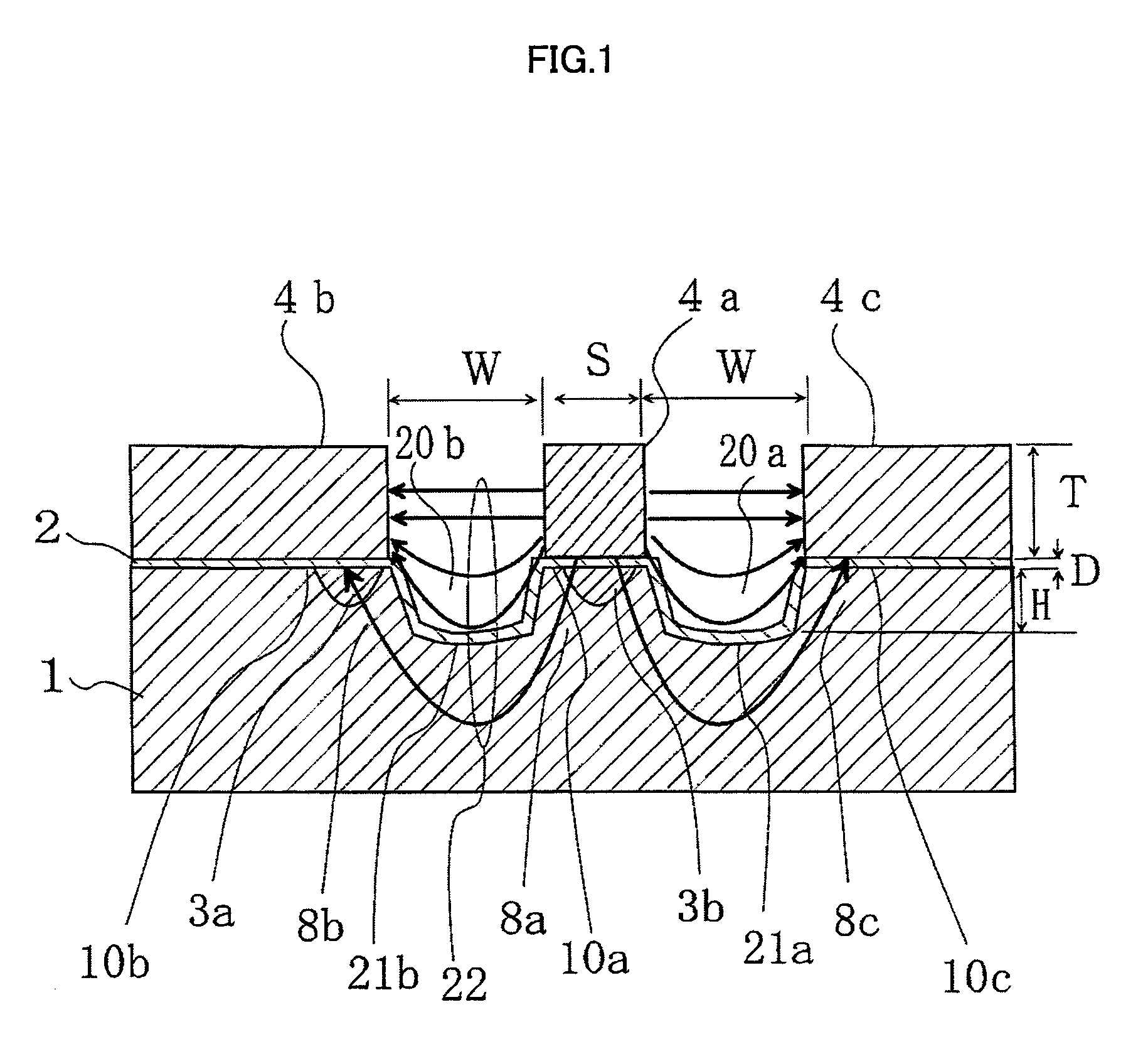
[0056]FIG. 1 is a sectional view schematically showing the optical modulator according to the first embodiment of the present invention. In this embodiment, the z-cut LN substrate 1 is not etched with dry etching method at the portions below the ground electrodes 4b and 4c, which is different from the optical modulator according to the second prior art shown in FIG. 12. However, it goes without saying that the z-cut LN substrate 1 may be etched at the portions below the ground electrodes 4b and 4c.

[0057]According to this first embodiment, the width “S” of the center electrode 4a is set at 9 μm, the gap “W” between the center electrode 4a and each of the ground electrodes 4b and 4c is set at 30 μm, the thickness “T” of the center electrode 4a and ground electrodes 4b and 4c is set at 18 μm, the height “H” of the ridge portion is set at 3 μm, and the thickness “D” of the SiO2 buffer layer 2 at the bottom surfaces 21a and 21b between the ridge portions and at the top parts 10a to 10c ...

second embodiment

[0075]Referring now to FIG. 7 of the accompanying drawings, an optical modulator according to the second embodiment of the present invention will be described hereinafter.

[0076]The constitutional elements of the second embodiment shown in FIG. 7 the same as those of the first embodiment of the optical modulator will not be described but bear the same reference numerals and legends as those of the first embodiment of the optical modulator.

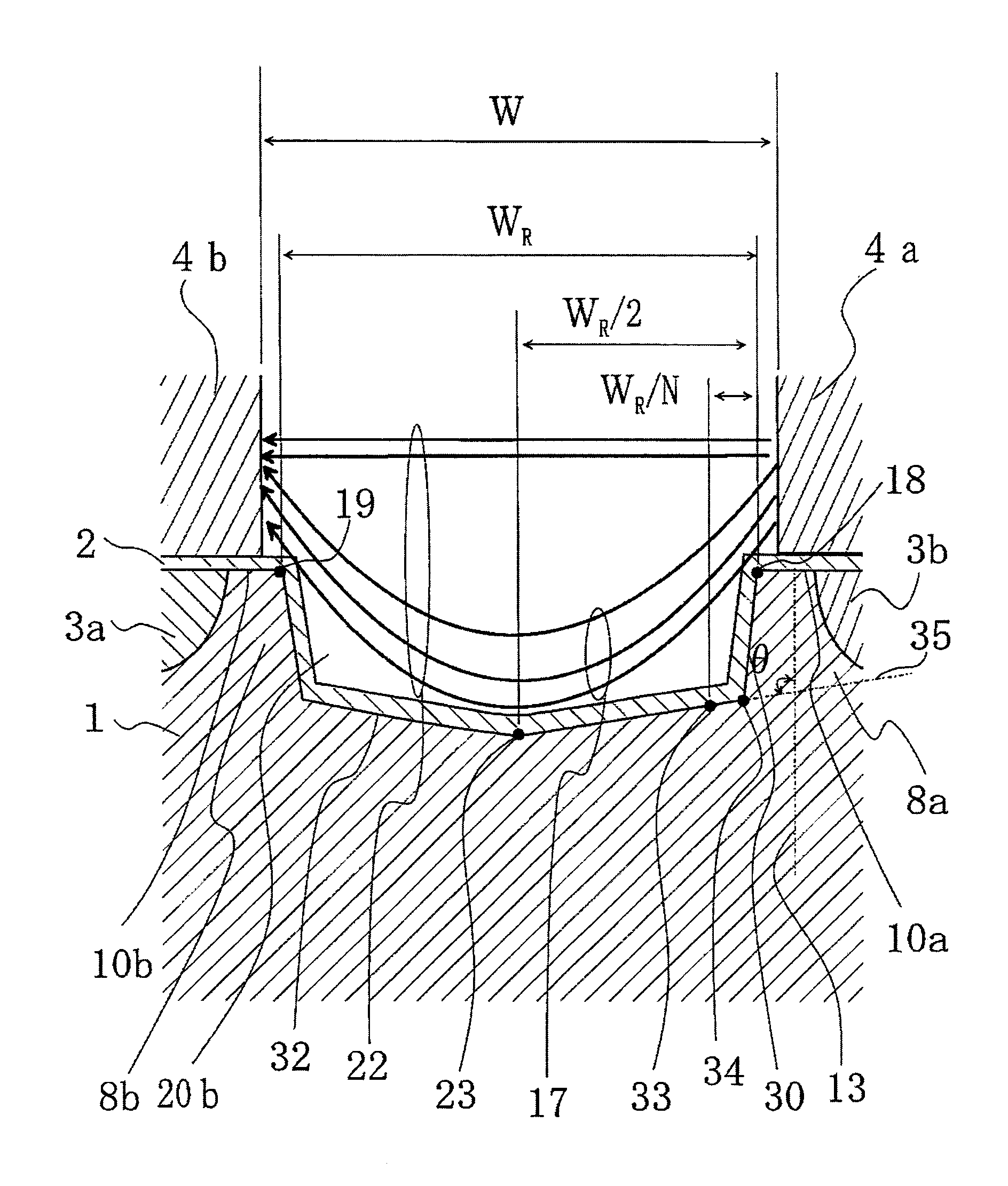
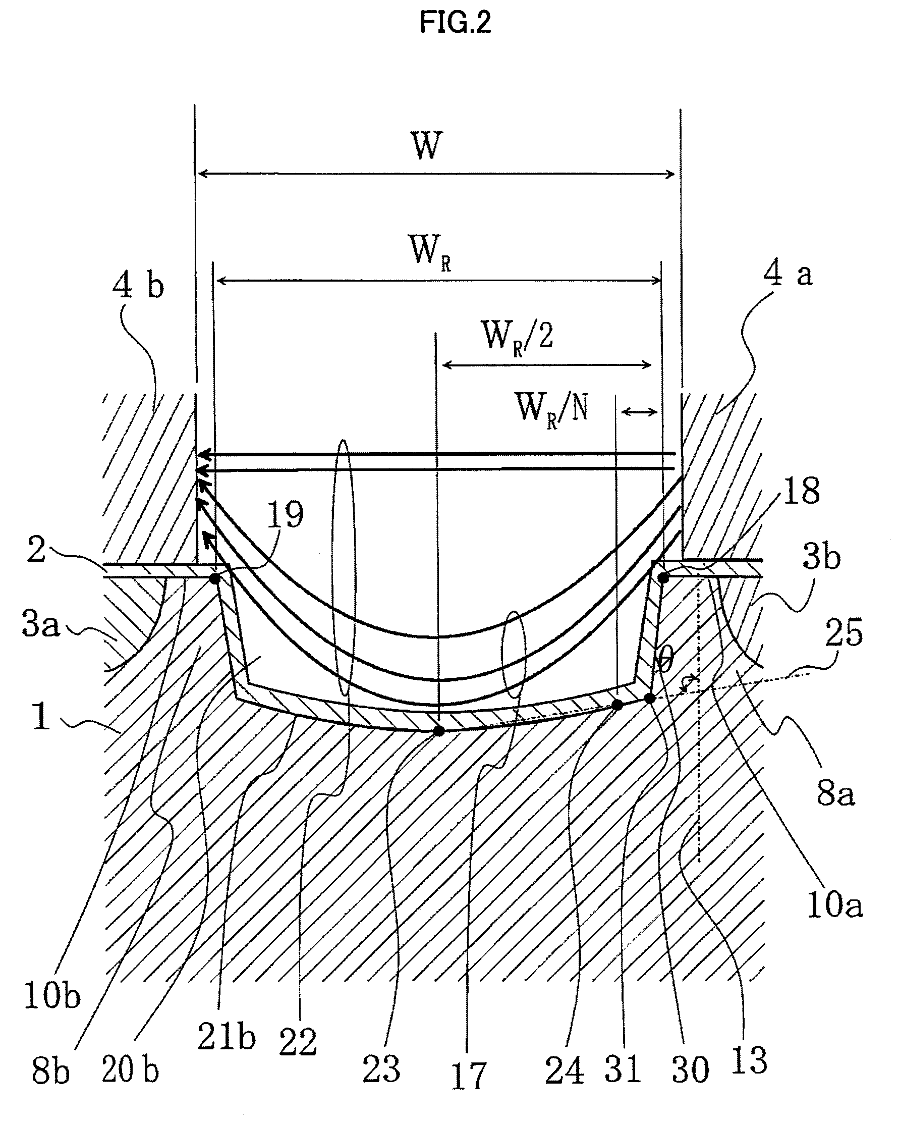
[0077]FIG. 7 is an enlarged view showing the optical modulator according to the second embodiment of this invention. In this embodiment, the line 25 passing through the center point 23 and the midway point 24 is crossed at an angle θ larger than 90.1° with the normal line 13 to the top part 10a of the ridge portion 8a. In this second embodiment, portions 26 and 27, proximity to the intersections defined by the bottom surface 21b and the respective ridge portions 8a and 8b, have a curvature with the radius of “R”. It is preferable that the radius “R”...

third embodiment

[0078]Referring now to FIG. 8 of the accompanying drawings, an optical modulator according to the third embodiment of the present invention will be described hereinafter.

[0079]The constitutional elements of the third embodiment shown in FIG. 8 the same as those of the above mentioned embodiments of the optical modulator will not be described but bear the same reference numerals and legends as those of the above mentioned embodiments of the optical modulator.

[0080]FIG. 8 is an enlarged view showing the optical modulator according to the third embodiment of this invention. In this third embodiment, the optical modulator is characterized by the fact that most part of the bottom surface 32 between the ridge portions 8a, 8b is formed by an inclined flat surface. The bottom surface 32 between the ridge portions 8a and 8b has a center point 23 positioned with the distance of WR / 2 in a horizontal direction from the end point 18 of the top part 10a of the ridge portion 8a below the center el...


PUM

PropertyMeasurementUnit
angleaaaaaaaaaa
curvature radiusaaaaaaaaaa
temperatureaaaaaaaaaa

Abstract

Herein disclosed is an optical modulator, having: a substrate (1); and a center and ground electrodes (4a to 4c), in which the substrate has ridge portions (8a to 8c), the center and ground electrodes are respectively formed above the ridge portions, the ridge portions below the center and ground electrodes respectively have top parts (10a, 10b) having a respective first and second end points (18, 19) separated with a distance of “WR”, the substrate has a bottom surface (21b) between the ridge portions having center and midway points (23, 24) positioned with a respective distance of WR / 2 and WR / N (3≦N≦25) from the first end point, the ridge portion below the center electrode has a normal line (13), and the center point and the midway point define a straight line (25) crossed with the normal line at an angle larger or equal to 90.1°.

Description

RELATED APPLICATIONS[0001]This application claims the benefit under 35 U.S.C. §119(e) of Provisional Patent Application Ser. No. 61 / 056,296 filed on May 27, 2008, the contents of which are incorporated by reference.FIELD OF THE INVENTION[0002]The present invention relates to an optical modulator for modulating, with high frequency electric signal, an incident light in an optical waveguide to be outputted as an optical pulse signal.DESCRIPTION OF THE RELATED ART[0003]In recent years, there has been practically used an optical communication system with high speed and high capacity. Many requests have been made to develop an optical modulator with high volume, small size and low cost for the purpose of enabling the optical modulator to be embedded in the optical communication system with high speed and high capacity.[0004]In response to these requests, there have so far been developed various types of optical modulators one of which is a traveling wave electrode type of lithium niobate...

Claims


Application Information

Patent Timeline
Patent Type & Authority Patents(United States)
IPC IPC(8): G02F1/035
CPCG02F1/2255G02F2001/212G02F1/212
Inventor KAWANO, KENJIUCHIDA, SEIJIKAWAZURA, EIJISATO, YUJINANAMI, MASAYANAKAHIRA, TORUIGARASHI, NOBUHIROMATSUMOTO, SATOSHI
Owner ANRITSU CORP
Why Eureka
Try Eureka