UV treatment of etch stop and hard mask films for selectivity and hermeticity enhancement

a technology of selectivity and hermeticity, applied in the field of forming a dielectric, can solve the problems of limiting the improvement of device performance, reducing manufacturing costs, and undesirable moisture penetration in a dielectric layer, and achieve the effect of increasing density and increasing selectivity and hermeticity

Active Publication Date: 2012-08-14
NOVELLUS SYSTEMS
View PDF209 Cites 356 Cited by
  • Summary
  • Abstract
  • Description
  • Claims
  • Application Information

AI Technical Summary

Benefits of technology

[0010]The present invention provides a method for the ultra-violet (UV) treatment of etch stop and hard mask films to increase etch selectivity and hermeticity by removing hydrogen, cross-linking the film, and increasing density. The UV exposure may be direct or through another dielectric layer and may be concurrent with thermal energy treatment (heating or annealing of the wafer). The method is particularly applicable in the context of damascene processing.

Problems solved by technology

As integrated circuits (IC) feature sizes shrink, problems of increased resistance and resistance-capacitance (RC) coupling offset any speed advantage derived from the smaller device size, limiting improvement in device performance.
Further, thinner films use less material and machine time, decreasing manufacturing costs.
Moisture is ubiquitous during semiconductor manufacture, but moisture penetration in a dielectric layer is undesirable.
Penetration by moisture is one of the hardest things to prevent, since the water molecule diffuses rapidly through many dielectrics.
In general, moisture penetration in dielectric films causes an increase in dielectric constant that degrades device performance.
It also causes reliability problems such as reduction in electromigration lifetime, enhanced stress migration and reduced Time Dependent Dielectric Breakdown (TDDB) for a number of reasons among which are poor adhesion, increased line-to-line leakage, metal oxidation and corrosion of the copper lines.
The presence of mobile fluorine and hydrogen leads to the eventual formation of HF, which causes adhesion problems and subsequent blistering of the dielectric films.
The moisture will also change the stress characteristics of the dielectric film, causing unwanted stress drift.

Method used


Image

  • UV treatment of etch stop and hard mask films for selectivity and hermeticity enhancement
  • UV treatment of etch stop and hard mask films for selectivity and hermeticity enhancement
  • UV treatment of etch stop and hard mask films for selectivity and hermeticity enhancement

Examples


Embodiment Construction

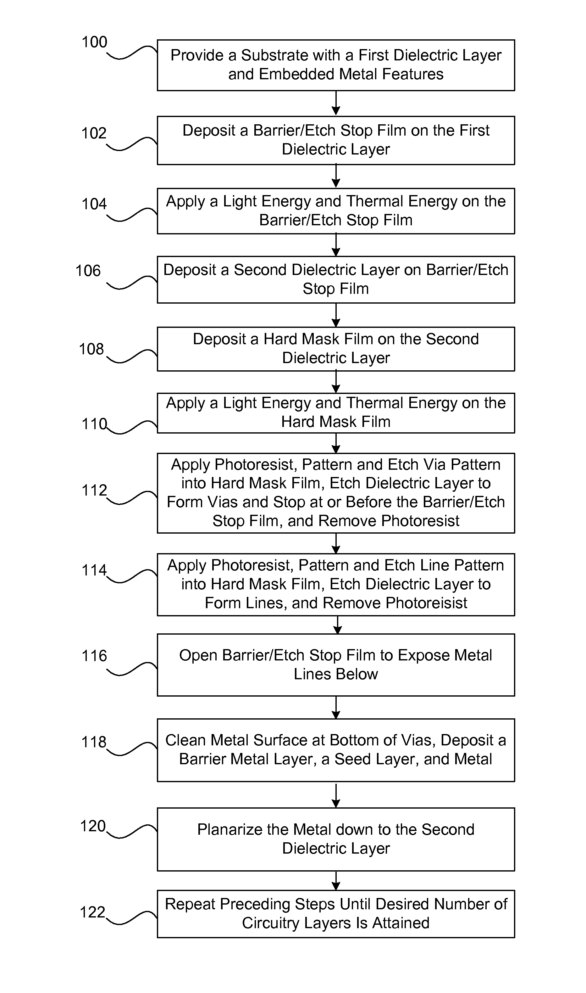
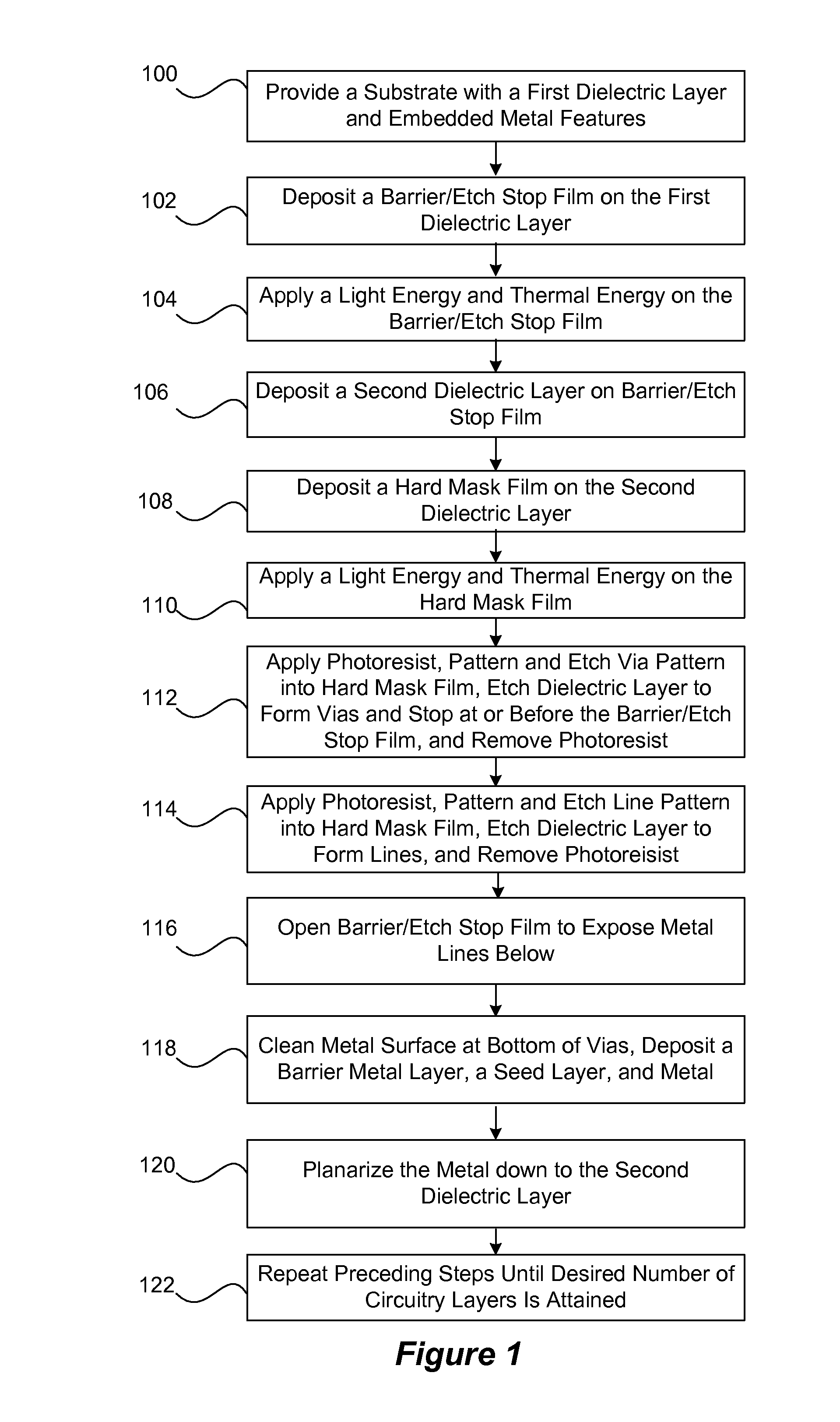
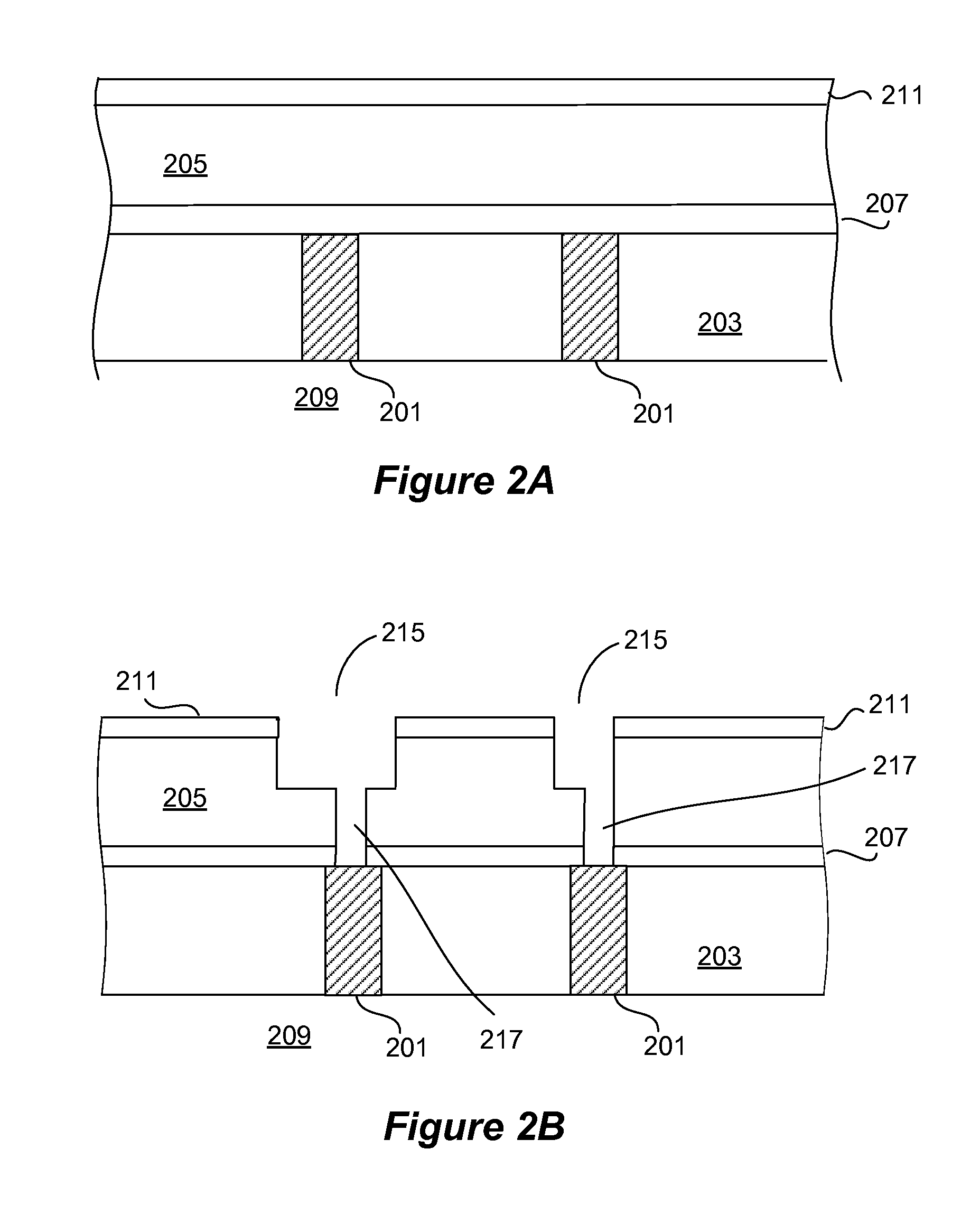
[0020]Embodiments of the present invention are described herein in the context of a UV treatment for etch stop or hard mask films in damascene processing. Those skilled in the art will realize that the following detailed description of the present invention is illustrative only and is not intended to be in any way limiting. Other embodiments of the present invention will readily suggest themselves to such skilled persons having the benefit of this disclosure. For example, although damascene processing is used in the discussion, the UV treatment of etch stop or hard mask films is effective in all applications where such films are used (e.g., aluminum interconnects).

[0021]Reference will be made in detail to implementations of the present invention as illustrated in the accompanying drawings. The same reference indicators will be used throughout the drawings and the following detailed description to refer to the same or like parts.

[0022]The term “semiconductor device” as used herein re...


PUM


Abstract

A method for the ultraviolet (UV) treatment of etch stop and hard mask film increases etch selectivity and hermeticity by removing hydrogen, cross-linking, and increasing density. The method is particularly applicable in the context of damascene processing. A method provides for forming a semiconductor device by depositing an etch stop film or a hard mask film on a substrate and exposing the film to UV radiation and optionally thermal energy. The UV exposure may be direct or through another dielectric layer.

Description

BACKGROUND OF THE INVENTION[0001]The present invention is related to a method of forming a dielectric of the type used in semiconductor applications, and more particularly to a process for improving selectivity and hermeticity characteristics of etch stop films and hard mask layers using UV treatment.[0002]As integrated circuits (IC) feature sizes shrink, problems of increased resistance and resistance-capacitance (RC) coupling offset any speed advantage derived from the smaller device size, limiting improvement in device performance. Ways to improve device performance and reliability include using highly conductive metals, such as copper, and employing lower dielectric constant (low-k) materials.[0003]Low-k materials are, by definition, those semiconductor-grade insulating materials that have a dielectric constant (“k”) lower than that of SiO2, i.e., 3.9. Various types of low-k materials can have dielectric constants ranging for instance from about 3.5-3.9 (e.g., FSG), to less than...

Claims


Application Information

Patent Timeline
Patent Type & Authority Patents(United States)
IPC IPC(8): H01L21/31H01L21/00H01L21/469
CPCH01L21/3105H01L21/31111H01L21/31144H01L21/76807H01L21/76825H01L21/76828H01L21/76829H01L21/76834
Inventor VAN SCHRAVENDIJK, BARTDENISSE, CHRISTIAN
Owner NOVELLUS SYSTEMS
Why Eureka
Try Eureka