In-situ wafer processing system and method

a technology of wafer processing and in-situ wafers, applied in the field of wafers, can solve the problems of increasing the amount of heat generated during slicing, requiring a much longer time to cut, and current wire saws generate heat, so as to increase the breakage rate of wafers, increase the cost of producing solar cells, and increase the wafer throughput

Inactive Publication Date: 2012-09-11
CAMBRIDGE ENERGY RESOURCES
View PDF55 Cites 7 Cited by
  • Summary
  • Abstract
  • Description
  • Claims
  • Application Information

AI Technical Summary

Benefits of technology

[0014]Typically, in the manufacture of wafers and cells for photovoltaic applications, thousands of wafers are processed per hour, which necessitates installing a large number of chemical stations to achieve a desired throughput. Thus, increasing the number of wafers per carrier / holder can significantly increase wafer throughput. Further, during the chemical etching process, thin wafers tend to float to the top surface of the etching solution, thereby resulting in not completely treating the wafers.
[0015]Furthermore, during diffusion and coating processes, the gases are blown over the thin wafers. The force generated by the blown gases can dislodge the wafers from the wafer carrier affecting productivity. Moreover, the above problems can become very acute when wafer thicknesses are reduced to 100 um (micrometer) or thinner. It can be seen that as the wafers and the subsequent solar cells become thinner, using the above described conventional process can significantly increase the breakage rate of wafers. This can result in increased cost for producing solar cells.

Problems solved by technology

This is particularly true for very thin wafers, which require a much longer time to cut.
In addition, the current wire saws generate heat during slicing.
Also, as the wafers become thinner, the cutting surface area increases significantly and as a result this can significantly increase the amount of heat generated during slicing.
Furthermore, lesser area is generally available for heat dissipation by radiation during slicing due to the slurry getting loaded between the wafers.
This can lead to significant thermal stress in the wafers.
This can result in wafers dislodging from the plate 160 and breaking during slicing.
Although the aforementioned conventional wire saws are widely used for slicing brittle materials such as silicon, they also impose a series of high stress operating conditions during slicing.
The wafers must withstand these forces during operation otherwise they will break.
This may pose serious challenge to the solar industry to slice thinner wafers.
As the silicon wafers are manufactured to thinner specification, the sensitivity of each wafer to any stress is increased and wafers readily break.
In summary, the mechanical, thermal and hydrodynamic stresses induced during the above slicing process can result in significant breakage of silicon wafers and thereby increasing the cost of manufacturing silicon wafers.
Further, as the silicon wafers are manufactured to thinner specifications, the sensitivity of these thinner wafers to any stress is significantly increased and these wafers can readily break.
Further, the slurry remaining between the wafers needs to be removed quickly otherwise the slurry between the wafer can harden and hold the wafers together tightly and can make it difficult to remove the wafers from the plate 160 and in some instances can break the wafers.
Furthermore, removing the wafers from the plate 160 is generally a very labor intensive task as the glue which holds the wafers to the plate 160 is softened by heating and also that the wafers are removed individually (mostly manually).
This can be a tremendous amount of manual task.
Moreover, this labor intensive task can lead to certain amount of breakage of sliced wafers during manual handling.
It can be seen that the above solar manufacturing process is very labor intensive and slow.
Also, it can be seen that the above described solar manufacturing process may require a significant amount of equipments.
All these steps can be very time consuming and can carry tremendous risk of wafer breakage.
The number of wafers that can be held in each carrier / holder is typically limited by the gap needed to be maintained between wafers in the carrier / holder.
Further, during the chemical etching process, thin wafers tend to float to the top surface of the etching solution, thereby resulting in not completely treating the wafers.

Method used


Image

  • In-situ wafer processing system and method
  • In-situ wafer processing system and method
  • In-situ wafer processing system and method

Examples


Embodiment Construction

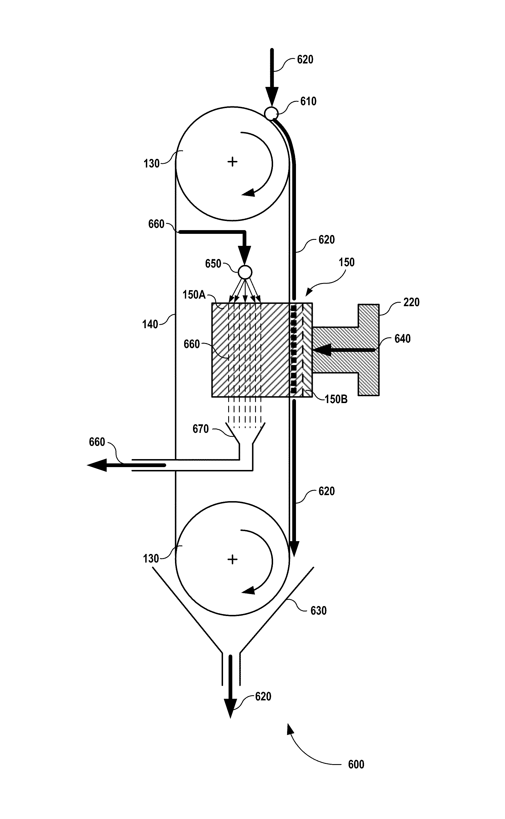
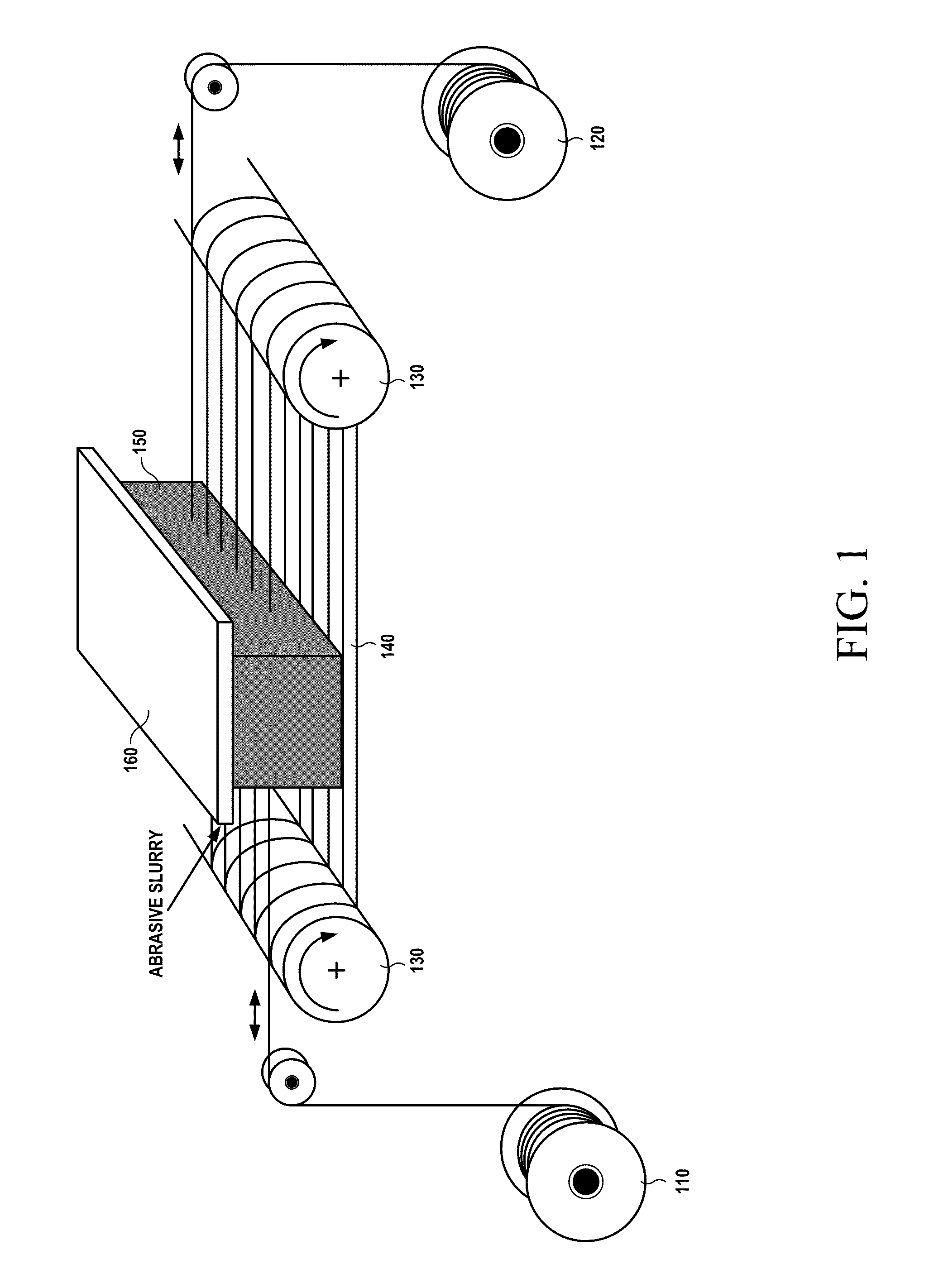
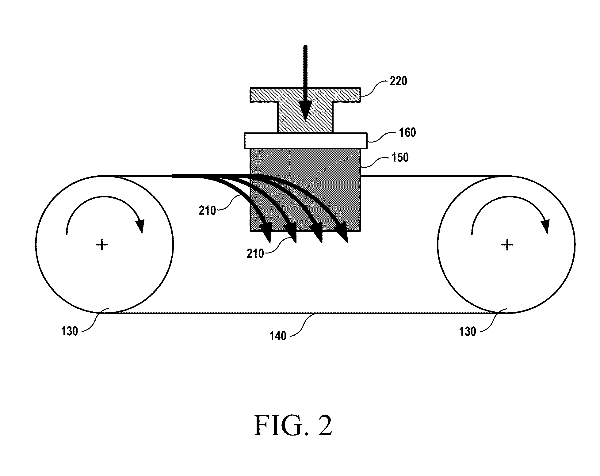
[0037]An integrated wafer processing system and a method thereof is disclosed. In the following detailed description of the embodiments of the invention, reference is made to the accompanying drawings that form a part hereof, and in which are shown by way of illustration specific embodiments in which the invention may be practiced. These embodiments are described in sufficient detail to enable those skilled in the art to practice the invention, and it is to be understood that other embodiments may be utilized and that changes may be made without departing from the scope of the present invention. The following detailed description is, therefore, not to be taken in a limiting sense, and the scope of the present invention is defined only by the appended claims.

[0038]The terms “slicing”, “sawing”, “watering”, and “cutting” are used interchangeably throughout the document. Also, the terms “sliced wafers” and “cut wafers” means the same. Further, the terms “integrated wafer processing sys...


PUM

PropertyMeasurementUnit
thicknessaaaaaaaaaa
thicknessaaaaaaaaaa
thicknessaaaaaaaaaa

Abstract

An integrated wafer processing system and a method thereof is disclosed. In one embodiment, a wafer stack of sliced wafers includes a base, and a plurality of sliced wafers extending outwardly from the base, where the plurality of sliced wafers are obtained by slicing a portion of a work piece, where the base is an uncut portion which is the remaining portion of the work piece or a plate attached by welding to the plurality of sliced wafers and where the work piece is mono-crystalline or multi-crystalline silicon. Further, the wafer stack of sliced wafers are treated in-situ in cleaning and wet chemical tanks for processes such as damage etching, texturization and oxide etching and also treated in-situ in high temperature furnaces for processes such as diffusion and anti-reflection coating.

Description

RELATED APPLICATIONS[0001]This application claims priority under 35 U.S.C. 119 to U.S. Provisional Application No. 61 / 117,609, entitled “INTEGRATED WAFER PROCESSING SYSTEM” by Cambridge Energy Resources, Inc., filed on Nov. 25, 2008, which is incorporated herein its entirety by reference.FIELD OF TECHNOLOGY[0002]The present invention relates generally to wafers and more particularly relates to system and method of manufacture of wafers and cells for photovoltaic applications.BACKGROUND[0003]Typically, manufacture of wafers and solar cells, include processes, such as slicing, cleaning, damage etching, texturization, diffusion, oxide etching, anti-reflection coating, metallization and so on. The slicing process is generally the first step in any solar cell manufacturing line. Wire saws are extensively used to slice crystalline silicon blocks to produce wafers.[0004]Besides slicing silicon, the wire saws are also used for slicing a variety of other materials including sapphire, gallium...

Claims


Application Information

Patent Timeline
Patent Type & Authority Patents(United States)
IPC IPC(8): B28D1/06
CPCB08B3/02B28D5/007B28D5/0076B28D5/0082B28D5/045B08B2203/0229Y02P70/10
Inventor BAKSHI, ABHAYA KUMARPANIGRAHI, BHASKAR CHANDRA
Owner CAMBRIDGE ENERGY RESOURCES
Why Eureka
Try Eureka