

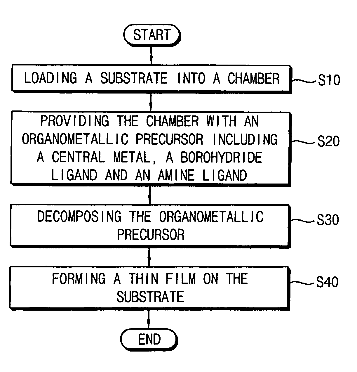
Organometallic precursor, thin film having the same, metal wiring including the thin film, method of forming a thin film and method of manufacturing a metal wiring using the same
a technology of organometallic precursors and thin films, applied in the direction of boron compounds, transportation and packaging, boron compounds, etc., can solve the problems of not substantially reducing the vaporization rate of organometallic precursors, and achieve the effects of reducing molecular interactions, reducing polarity, and reducing the interaction between molecules of organometallic precursors
- Summary
- Abstract
- Description
- Claims
- Application Information
AI Technical Summary
Benefits of technology
Problems solved by technology
Method used
Image

Examples
example 1
[0079]About 453.32 g of aluminum chloride (AlCl3) was diluted with about 2 L of ethyl ether and about 180.63 g of lithium aluminum hydride (LiAlH4) was diluted with about 1.5 L of ethyl ether. Reactants were cooled to a temperature of about −30° C. The solution including aluminum chloride was added to the solution including lithium aluminum hydride, and was mixed together. About 401.91 g of N,N-dimethylethylamine (NEtMe2) was added to the solution including aluminum chloride and lithium aluminum hydride. The reaction was carried out for about five hours. The solution including a reaction product, ClAlH2NEtMe2, was filtered. About 514.44 g of sodium borohydride (NaBH4) was diluted with about 2 L of ethyl ether. The solution including ClAlH2NEtMe2 was dropped into the sodium borohydride solution for about 30 minutes. The mixture was reacted for about 20 hours, and filtered to remove solvent from the mixture. The filtered resultant was purified by a vacuum evaporation. As a result, a c...
PUM
| Property | Measurement | Unit |
|---|---|---|
| temperature | aaaaa | aaaaa |
| temperature | aaaaa | aaaaa |
| electrical conductivity | aaaaa | aaaaa |
Abstract
Description
Claims
Application Information