

Method and apparatus for producing conductive material
a technology of conductive materials and apparatuses, which is applied in the direction of liquid/solution decomposition chemical coating, photomechanical equipment, instruments, etc., can solve the problems of deterioration of light transmittance and image quality, increased waste liquid treatment cost, and inability to form printed wires with a small width easily, so as to improve visibility, reduce light reflection, and improve the effect of fluidity
- Summary
- Abstract
- Description
- Claims
- Application Information
AI Technical Summary
Benefits of technology
Problems solved by technology
Method used
Image

Examples
example 1
Preparation of Conductive Base Material A)
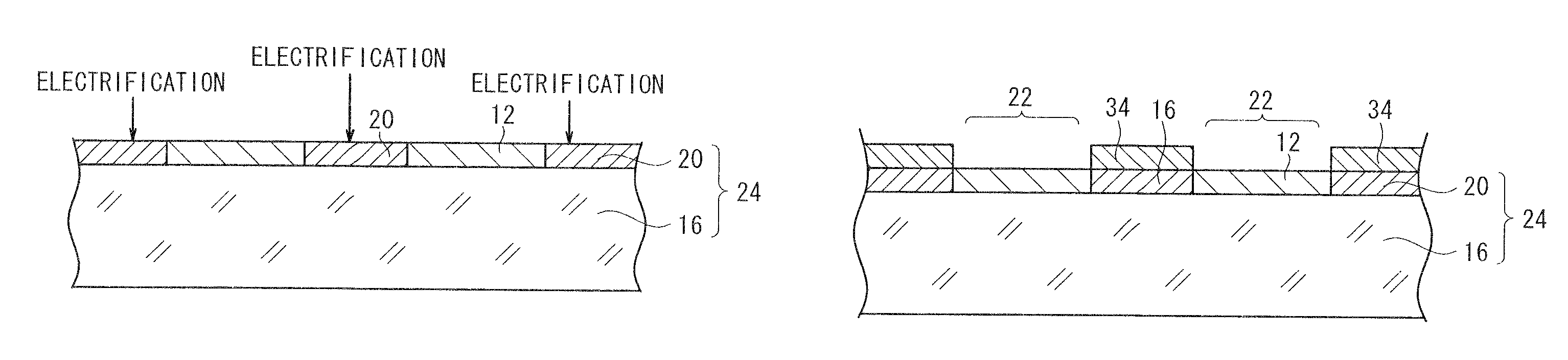
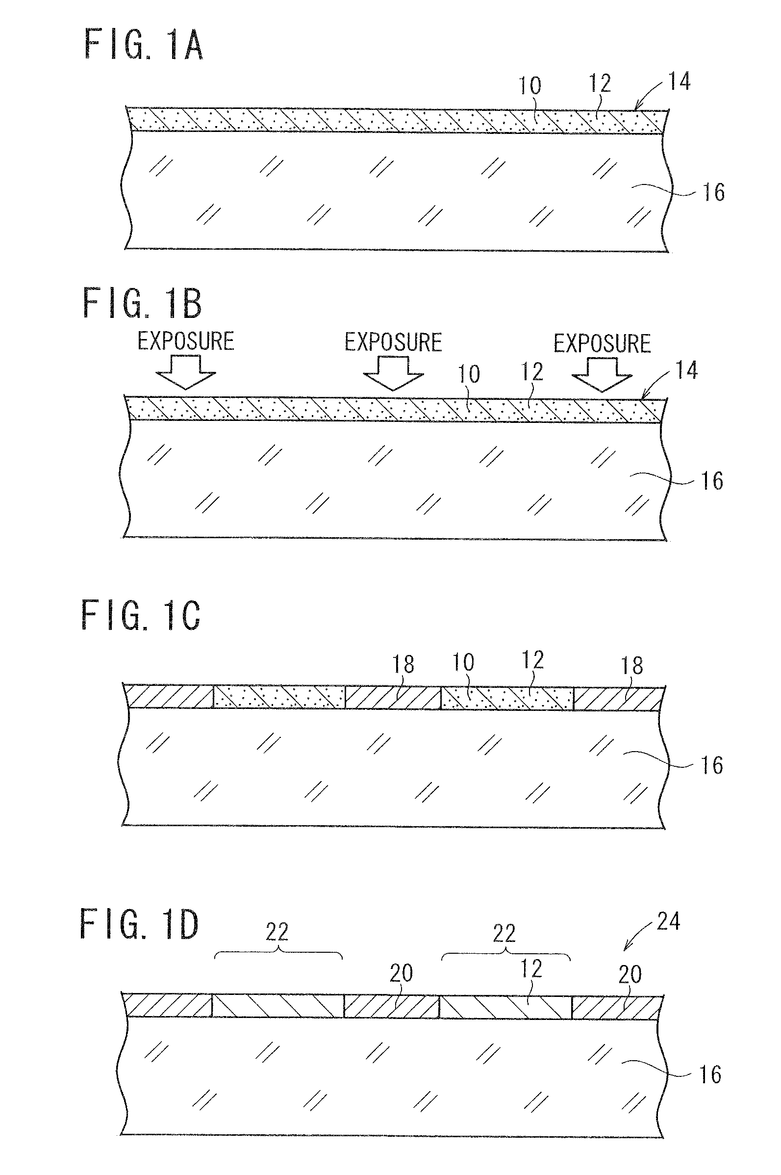
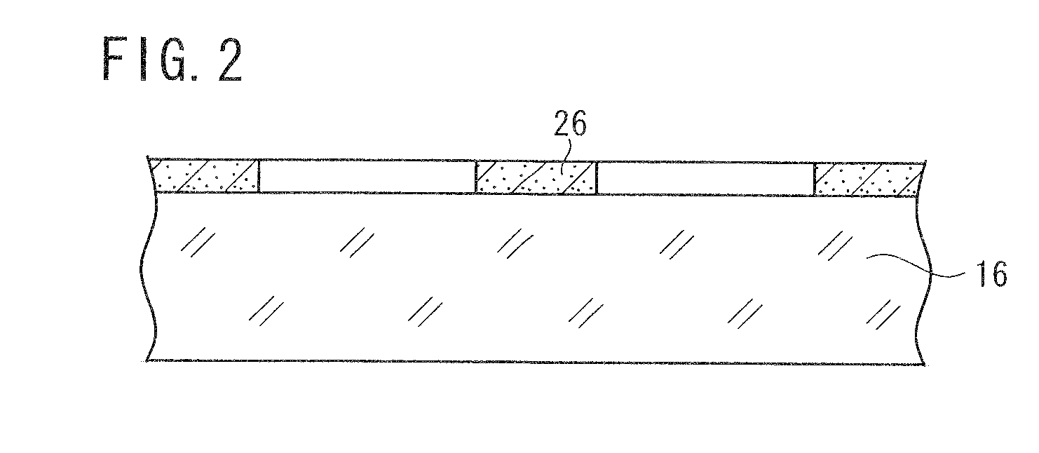
[0156]A base material was prepared by the following procedure, and coated with a photosensitive silver halide material. The photosensitive silver halide material was exposed in a mesh pattern and developed, whereby conductive fine particles of developed silver were deposited on the base material. The conductive fine particles formed a mesh pattern of lines, which were disposed at a regular interval at angles of 45° and 135° against the longitudinal direction of the ribbon-shaped base material. The mesh pattern had a line width of 12 μm and a space width of 288 μm. Thus obtained conductive base material is referred to as a conductive base material A. The conductive base material A had a surface resistance of 200 Ω / sq and a transmittance of 85% to a D65 light source. The surface resistance was measured by LORESTA GP manufactured by Mitsubishi Chemical Corporation, utilizing a four-probe method.
[0157]The emulsion surface and back surface of a b...
example 2
Conductive Materials Were Produced and Evaluated as Follows
(Production of Sample 2-1)
[0203]A sample 2-1, a conductive material according to the present invention, was produced in the same manner as the sample 1-1 of Example 1 except for adding 30 mg / L of sodium chloride, 100 mg / L of PEG1000, 10 mg / L of Janus green B, and 10 mg / L of bis(3-sulfopropyl) disulfide to the activation solution.
(Production of Samples 2-2 to 2-17)
[0204]Samples 2-2 to 2-17 were produced respectively in the same manner as the sample 2-1 except for changing the metal ion content, the complexing agent content, and the pH and the electrification conditions of the activation solution to those shown in Table 2. The pH was controlled by addition of NaOH or sulfuric acid. The produced samples were evaluated in terms of the following values.
(Surface Resistance)
[0205]The surface resistance of each sample was measured in the same manner as in Example 1 after the electroless plating.
(Roughness)
[0206]After the electroless...
example 3
[0211]Conductive materials could be produced in the same manner as the samples 1-1 and 1-6 of Example 1 except for changing the above electroless plating solutions to the following nickel plating solutions.
[0212]
(Electroless nickel plating solution composition andelectroless nickel plating condition)Nickel sulfate25 g / LSodium hypophosphite20 g / LSodium acetate10 g / LSodium citrate10 g / LpH5.0Treatment temperature90° C.
PUM
| Property | Measurement | Unit |
|---|---|---|
| diameter | aaaaa | aaaaa |
| current density | aaaaa | aaaaa |
| electrifying time | aaaaa | aaaaa |
Abstract
Description
Claims
Application Information