Nonvolatile memory element and nonvolatile memory device

a non-volatile memory and element technology, applied in semiconductor devices, digital storage, instruments, etc., can solve the problem that the limit of the miniaturization of flash memories using existing floating gates cannot meet such a demand, and achieve the effect of stable operation

Active Publication Date: 2012-10-02
PANASONIC SEMICON SOLUTIONS CO LTD
View PDF33 Cites 33 Cited by
  • Summary
  • Abstract
  • Description
  • Claims
  • Application Information

AI Technical Summary

Benefits of technology

[0026]With this, because the at least one of the following conditions is satisfied: (1) the dielectric constant of the second oxide layer is larger than that of the first oxide layer; and (2) the band gap of the second oxide layer is smaller than that of the first oxide layer, a strength of a breakdown electric field of the second oxide layer having a high resistivity is reduced more than that of the first oxide layer having a low resistivity. As a result, a breakdown voltage in the initial breakdown of the nonvolatile memory element (i.e., a nonvolatile memory element including a variable resistance layer having a stacked structure of transition metal oxide layers) which is in the high resistance state in the initial state is reduced, the second oxide layer including the second transition metal having a small standard electrode potential, that is, the second oxide layer being easy to oxidize among the first oxide layer and the second oxide layer included in the variable resistance layer.
[0028]It is to be noted that in the nonvolatile memory element according to the first aspect, the second electrode is preferably formed in contact with the second oxide layer, and a standard electrode potential of a material of the second electrode is preferably higher than the standard electrode potential of the second transition metal. With this, because a condition for causing a resistance change of an oxygen-deficient transition metal oxide layer (that is, the second oxide layer) is satisfied in the relationship between the oxygen-deficient transition metal oxide layer and its adjacent electrode, the resistance change of the nonvolatile memory element is assured, and a stable operation is achieved.
[0036]With this, because the nonvolatile memory device according to the second aspect includes the nonvolatile memory elements according to the present invention which have the above-described characteristics, the breakdown voltage of the initial breakdown of each nonvolatile memory element which is in the high resistance state in the initial state is reduced.
[0040]The nonvolatile memory element and the nonvolatile memory device according to the present invention allow the reduction in the breakdown voltage of the initial breakdown of the nonvolatile memory element and the reliable change of the resistance value of the nonvolatile memory element, and thus achieve the stable operation.

Problems solved by technology

It is said that miniaturization of flash memories using existing floating gates has a limit to meet such a demand.

Method used


Image

  • Nonvolatile memory element and nonvolatile memory device
  • Nonvolatile memory element and nonvolatile memory device
  • Nonvolatile memory element and nonvolatile memory device

Examples


embodiment 1

[0073]First, the following describes a nonvolatile memory element according to Embodiment 1 of the present invention.

[0074](Structure of Nonvolatile Memory Element)

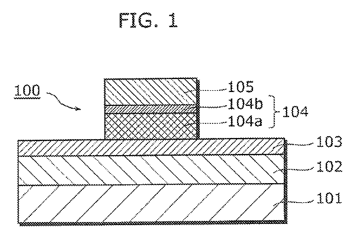
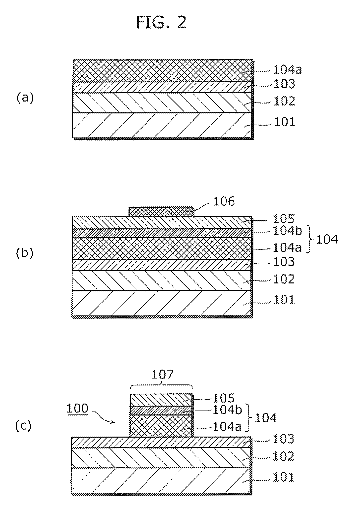
[0075]FIG. 1 is a cross-sectional view showing a structure of a nonvolatile memory element 100 according to Embodiment 1 of the present invention. As shown in FIG. 1, the nonvolatile memory element 100 is a variable resistance nonvolatile memory element, and includes a substrate 101, an oxide layer 102 formed on the substrate 101, a first electrode layer 103 formed on the oxide layer 102, a second electrode layer 105, and a variable resistance layer 104 formed between the first electrode layer 103 and the second electrode layer 105. The first electrode layer 103 and the second electrode layer 105 are electrically connected to the variable resistance layer 104.

[0076]The variable resistance layer 104 is a bipolar variable resistance layer whose resistance state reversibly changes between a high resistance state and a low re...

embodiment 2

[0153]Next, a nonvolatile memory device according to Embodiment 2 of the present invention shall be described.

[0154]The nonvolatile memory element 100 according to the above-mentioned Embodiment 1 can be applied to various forms of nonvolatile memory device. The nonvolatile memory device according to Embodiment 2 is a nonvolatile memory device including the nonvolatile memory element according to Embodiment 1, and is a so-called crosspoint nonvolatile memory device in which the nonvolatile memory element is interposed at a crosspoint (three-dimensional crosspoint) between a word line and a bit line.

[0155](Structure of Nonvolatile Memory Device)

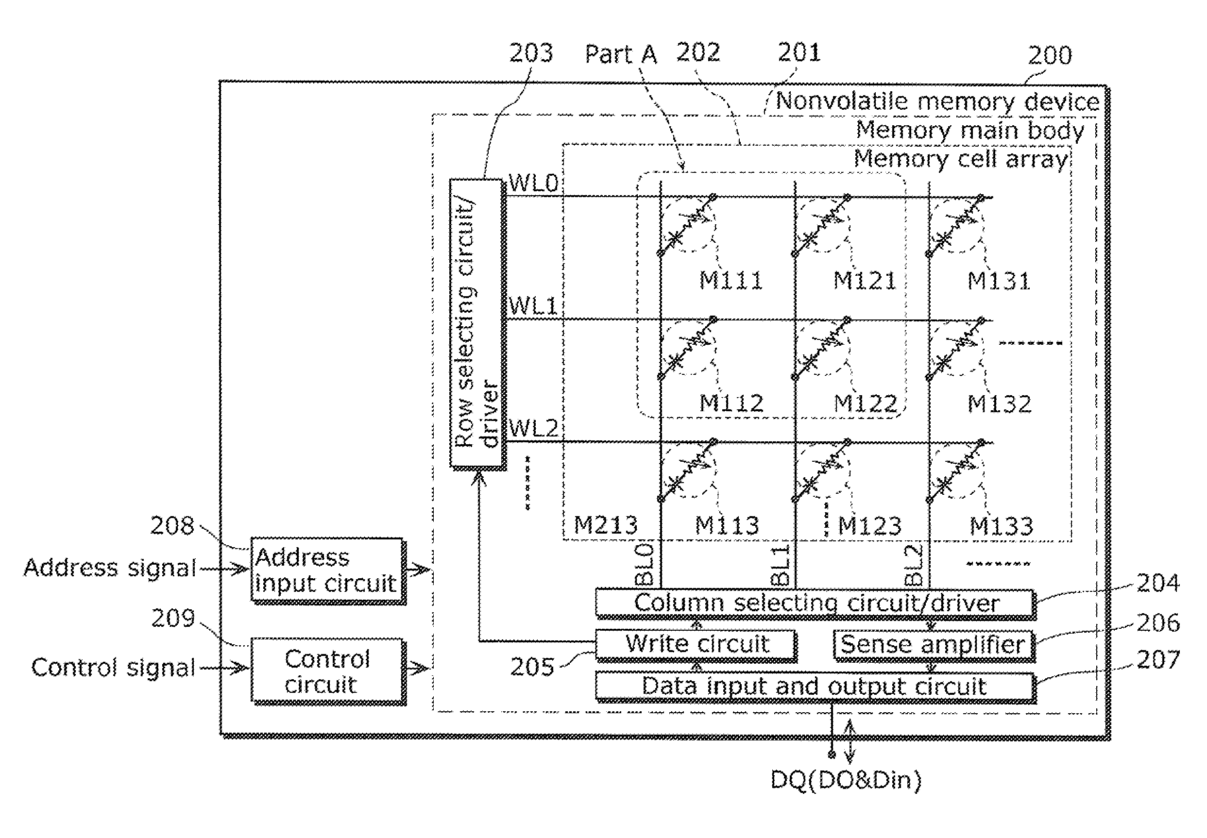
[0156]FIG. 25 is a block diagram showing a structure of a nonvolatile memory element 200 according to Embodiment 2 of the present invention. Furthermore, FIG. 26 is a perspective view showing a structure of part A (physical structure of a memory cell for four bits) shown in FIG. 25.

[0157]As shown in FIG. 25, the nonvolatile memory device 200 a...

embodiment 3

[0185]Next, a nonvolatile memory device according to Embodiment 3 of the present invention shall be described.

[0186]The nonvolatile memory device according to Embodiment 3 is a nonvolatile memory device including the nonvolatile memory element 100 according to Embodiment 1, and is a so-called 1T1R nonvolatile memory device in which a unit memory includes one transistor and one nonvolatile memory unit.

[0187](Structure of Nonvolatile Memory Device)

[0188]FIG. 29 is a block diagram showing a structure of a nonvolatile memory element 300 according to Embodiment 3 of the present invention. Furthermore, FIG. 30 is a perspective view showing a structure of part C (physical structure of a memory cell for two bits) shown in FIG. 29.

[0189]As shown in FIG. 29, the nonvolatile memory device 300 according to the present embodiment includes a memory main body 301 on a semiconductor substrate. The memory main body 301 includes: a memory cell array 302; a row selection circuit / driver 303, a column s...


PUM


Abstract

Provided is a nonvolatile memory element which is capable of performing a stable resistance change operation at a low breakdown voltage.A nonvolatile memory element (100) includes: a first electrode layer (103); a second electrode layer (105); and a variable resistance layer (104) which is placed between the electrodes (103 and 105), and whose resistance state reversibly changes between a high resistance state and a low resistance state based on a polarity of a voltage applied between the electrodes (103 and 105). The variable resistance layer (104) is formed by stacking a first oxide layer (104a) including an oxide of a first transition metal and a second oxide layer (104b) including an oxide of a second transition metal which is different from the first transition metal. At least one of the following conditions is satisfied: (1) a dielectric constant of the second oxide layer (104b) is larger than a dielectric constant of the first oxide layer (104a); and (2) a band gap of the second oxide layer (104b) is smaller than a band gap of the first oxide layer (104a).

Description

TECHNICAL FIELD[0001]The present invention relates to a nonvolatile memory element, and in particular to a so-called variable resistance nonvolatile memory element whose resistance state reversibly changes between a high resistance state and a low resistance state based on a polarity of an applied voltage, and a nonvolatile memory device including the nonvolatile memory element.BACKGROUND ART[0002]With the development of digital technology, electronic devices such as mobile information devices and home information appliances have become increasingly highly functional in recent years. Thus, we have seen a rise in the demand for nonvolatile memory elements which have larger capacity, allow power reduction in writing, reduce writing and reading time, and have longer operating life.[0003]It is said that miniaturization of flash memories using existing floating gates has a limit to meet such a demand. On the other hand, in the case of a variable resistance nonvolatile memory element in w...

Claims


Application Information

Patent Timeline
Patent Type & Authority Patents(United States)
IPC IPC(8): G11C11/00
CPCG11C13/0007G11C13/0069H01L27/101H01L45/1625H01L45/1675H01L45/08H01L45/1233H01L45/146H01L27/2409H01L27/2436H01L27/2463G11C2013/0073G11C2013/0083G11C2213/31G11C2213/32G11C2213/56H10B63/20H10B63/30H10B63/80H10N70/24H10N70/826H10N70/8833H10N70/026H10N70/063
Inventor TAKAGI, TAKESHIWEI, ZHIQIANGNINOMIYA, TAKEKIMURAOKA, SHUNSAKUKANZAWA, YOSHIHIKO
Owner PANASONIC SEMICON SOLUTIONS CO LTD
Why Eureka
Try Eureka