Spin polarised magnetic device

a magnetic device and spin polarisation technology, applied in the direction of solid-state devices, magnetic bodies, instruments, etc., can solve the problems of increasing the number of address errors, affecting selectivity, and the writing mechanism described above presents some difficulties, so as to reduce the stochastic fluctuations in the magnetisation reversal time

Active Publication Date: 2012-10-02
INSTITUT NAT POLYTECHN DE GRENOBLE +2
View PDF4 Cites 127 Cited by
  • Summary
  • Abstract
  • Description
  • Claims
  • Application Information

AI Technical Summary

Benefits of technology

[0026]In this context, the purpose of this invention is to provide a magnetic device enabling the aforementioned requirements regarding the duration of current pulses crossing the device connected to the raised precession frequencies to be overcome, while reducing the stochastic fluctuations in the magnetisation reversal time and the critical current density for magnetisation reversal.

Problems solved by technology

However, the writing mechanism described above presents some difficulties.
The first problem is a problem regarding selectivity.
For high density memories, as the size of the memory points is clearly submicronic, the number of address errors increases.
This selectivity problem could be improved by introducing a writing technology referred to as “toggle” technology, described in the U.S. Pat. No. 6,545,906, however at the price of an increase in electrical consumption.
The critical current has been lowered by a factor of 3 due to this dual configuration; however this value still remains too high.
Moreover, this configuration does not resolve the problems of the stochastic fluctuations in the reversing or switching time.
However, as the spin transfer torque varies with the sine of the angle between the current polarisation and the magnetisation, the torque is initially zero with the effect that the switching is difficult to start.
In one memory or logic component mode of operation, this waiting time is particularly disadvantageous as it restricts the operating speed of the memory or component.
Moreover, this configuration does not resolve the problem of the stochastic fluctuations in the magnetisation reversing time.
In a memory chip-type electronic device, this is very difficult to achieve as the inductive and capacitive effects produced during the distribution of current pulses within the conducting lines causes delays and enlarged pulses.
These deformations of the electrical signal are detrimental for the implementation of this precessional switch in a memory device.
This causes an uncertainty in the time required for the magnetisation to switch, which is disadvantageous in the perspective of using this phenomenon for writing MRAM cells.

Method used


Image

  • Spin polarised magnetic device
  • Spin polarised magnetic device
  • Spin polarised magnetic device

Examples


Embodiment Construction

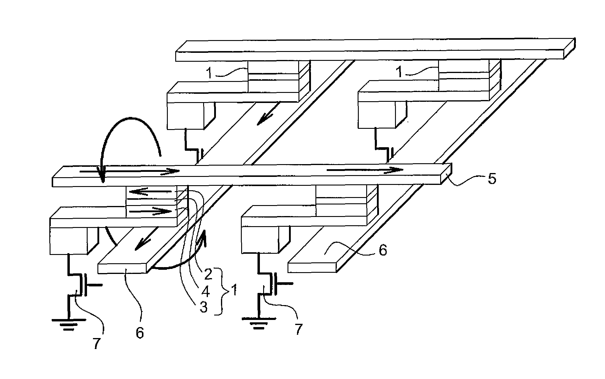
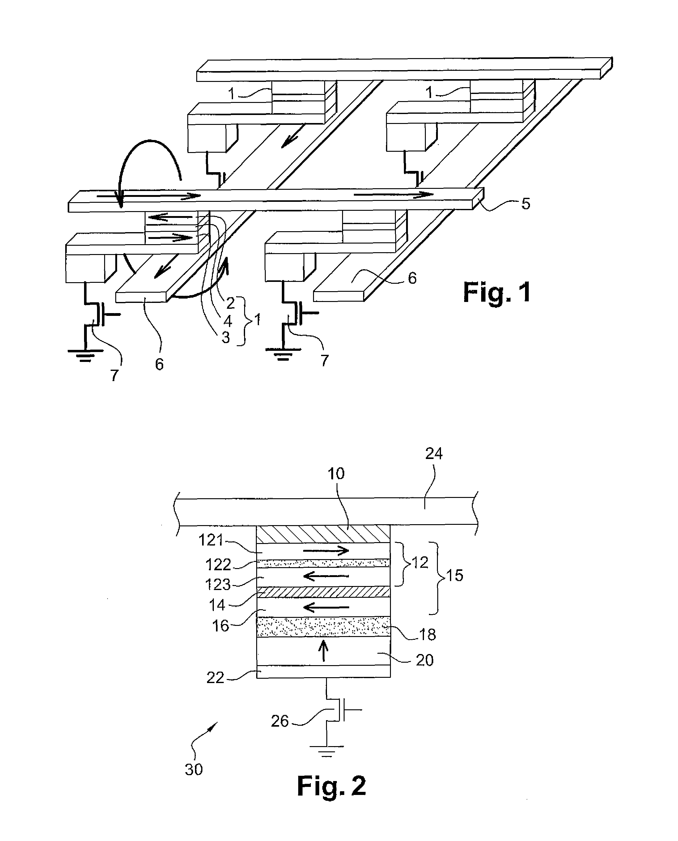
[0108]FIGS. 1 to 4 have already been described with reference to the state of the art.

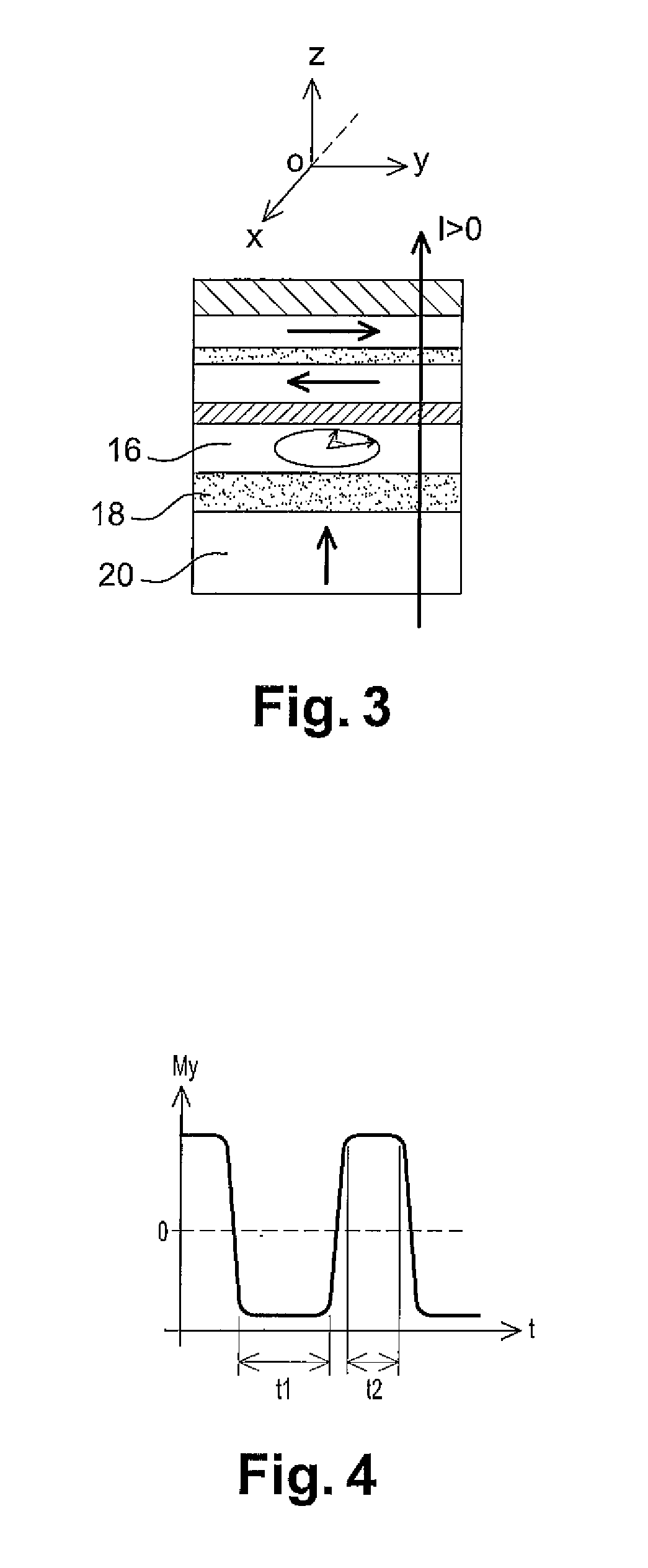
[0109]An Oxyz trirectangular trihedron enables the different directions to be located, the Oz axis being perpendicular to the plane of the layers.

[0110]FIG. 5 schematically represents a magnetic device 200 according to the invention.

[0111]The magnetic device 200 comprises:[0112]a magnetic reference layer 201 with a fixed magnetisation direction (in this case located in the plane of the reference layer);[0113]a first non-magnetic spacer 202;[0114]a magnetic storage layer 203 with a magnetisation capable of being redirected according to two substantially opposite states of direction (two positions of equilibrium substantially following the axis defined by the fixed magnetisation direction of the reference layer 201);[0115]a second spacer 204;[0116]a layer 205 generating spin polarised electrons with a magnetisation located out of the plane of the polarisation layer and with a direction perpendicular ...


PUM


Abstract

A magnetic device includes a magnetic reference layer with a fixed magnetization direction located either in the plane of the layer or perpendicular to the plane of the layer, a magnetic storage layer with a variable magnetization direction, a non-magnetic spacer separating the reference layer and the storage layer and a magnetic spin polarizing layer with a magnetization perpendicular to that of the reference layer, and located out of the plane of the spin polarizing layer if the magnetization of the reference layer is directed in the plane of the reference layer or in the plane of the spin polarizing layer if the magnetization of the reference layer is directed perpendicular to the plane of the reference layer. The spin transfer coefficient between the reference layer and the storage layer is higher than the spin transfer coefficient between the spin polarizing layer and the storage layer.

Description

CROSS-REFERENCE TO RELATED APPLICATIONS[0001]This application is based upon and claims the benefit of priority from French patent application Ser. No. 09 / 53512, filed May 27, 2009, the entire content of which is incorporated herein by reference.BACKGROUND[0002]1. Field[0003]This invention relates to a spin polarised magnetic device. This invention is applicable to the field of electronics, in particular for the production of memory points and MRAM (Magnetic Random Access Memory) type memory.[0004]2. Description of Related Art[0005]The context of the invention is that of MRAMs based on magnetic tunnel junctions (also referred to as magnetoresistive stacks) and more particularly MRAMs in which the writing operations are performed by spin transfer. FIG. 1 schematically illustrates the structure and function of such a junction bearing reference number 1. In a known manner, the magnetic tunnel junction (or magnetoresistive stack) 1 is comprised of two magnetic layers 2 and 3 separated by...

Claims


Application Information

Patent Timeline
Patent Type & Authority Patents(United States)
IPC IPC(8): G11C11/14
CPCB82Y25/00G11C11/16H01F10/3254H01L27/228H01F10/3286H01L43/10G01R33/093G01R33/1284H01L43/08G11C11/161H10B61/22H10N50/10H10N50/85
Inventor DIENY, BERNARDPAPUSOI, CRISTIANEBELS, URSULAHOUSSAMEDDINE, DIMITRIBUDA-PREJBEANU, LILIANASOUSA, RICARDO
Owner INSTITUT NAT POLYTECHN DE GRENOBLE
Why Eureka
Try Eureka