Fabrication of a microcantilever microwave probe

a technology of microwave probes and fabrication methods, which is applied in the field of microcantilever microwave probe fabrication, can solve the problems of inability to similarly anisotropically etch metals needed for microwave microscopy, inability to design microwave probes inherently more complicated, and difficulty in fabricating microwave probes, etc., and achieves enhanced shielding of the conducting path, low cost, and high yield

Active Publication Date: 2012-11-06
PRIMENANO
View PDF14 Cites 8 Cited by
  • Summary
  • Abstract
  • Description
  • Claims
  • Application Information

AI Technical Summary

Benefits of technology

[0009]In another aspect of the invention, a metal shield structure is developed on both sides of the cantilever sandwiching the conducting path together with intermediate dielectric layers to insulate the conducting path. Additionally, the backside metal shield may extend over the back of the metal probe tip with an intervening dielectric. Shielding of the conducting path is enhanced if the two shielding layers are at least two times and preferably four times the width of the conducting path.
[0011]In another aspect of the invention, the resistance of the conduction path and the path-to-shield capacitance are optimized to strengthen the microwave signal at the probe tip and the reflected microwave signal received by the detection circuitry. Preferably, the characteristic impedance of the transmission line is greater than 3 ohms and more preferably above 5 ohms.

Problems solved by technology

The design of the microwave probe is inherently more complicated than the relatively simple structure of an AFM probe for a number of reasons.
Such sharpness is often achieved by anisotropically etching crystalline silicon in an AFM probe, but metals needed for microwave microscopy cannot be similarly anisotropically etched.
Due to these problems and the necessary complexity of a microwave probe structure, the fabrication of microwave probes has proven to be difficult.
The most common design of the near-field microwave probe includes an etched metal tip, but metal etching limits the spatial resolution to no less than several micrometers.
Although diameters of FIB tips can be as small as 200 nm, such relatively large tips are too large for many applications in nano science and the characterization of nano materials.
Furthermore, the process of fabricating FIB-deposited tips is expensive and time consuming and this type of probe tip cannot be batched fabricated, that is, many tips simultaneously developed on a wafer and thereafter separated for use.

Method used


Image

  • Fabrication of a microcantilever microwave probe
  • Fabrication of a microcantilever microwave probe
  • Fabrication of a microcantilever microwave probe

Examples


Embodiment Construction

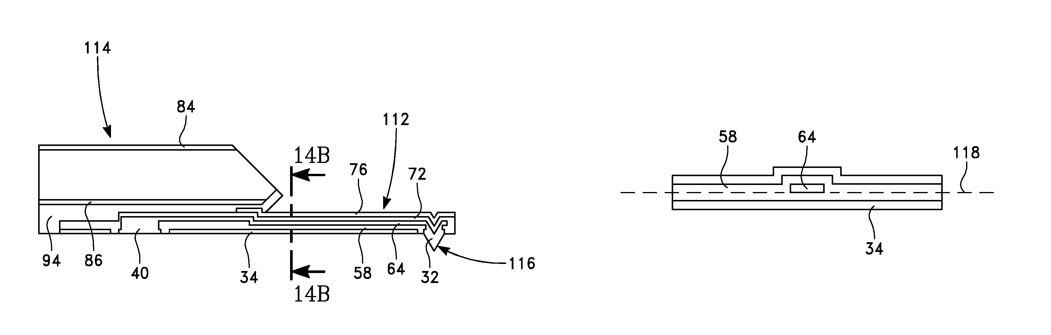
[0034]A first embodiment of a microwave probe includes a sharp metal tip projecting from a distal, free end of a cantilever. The proximal end of the cantilever is fixed to a support, also called a handle. A conduction path along the cantilever connects the metal tip to microwave electrical elements on the support.

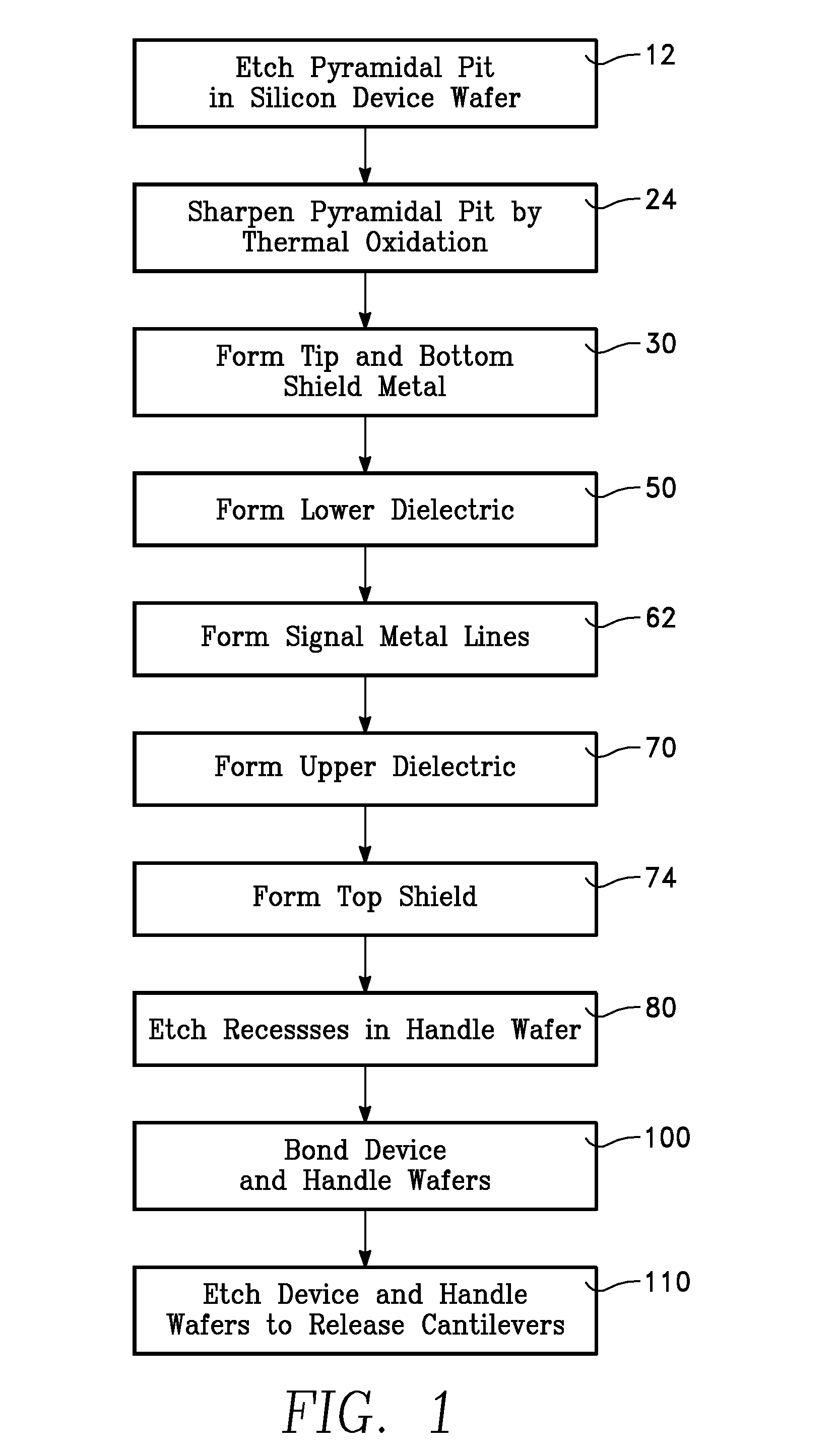
[0035]As a means of introduction, in one exemplary process for forming the microwave probe, the metal tip is developed in a crystalline device substrate and the cantilever and its metal and dielectric layers are formed in layers deposited on the device substrate and then patterned. The so developed device substrate is bonded to a handle substrate. The remnant portion of the device substrate is removed, and the support is patterned in the handle substrate. A more detailed process flow is presented in the flow diagram of FIG. 1.

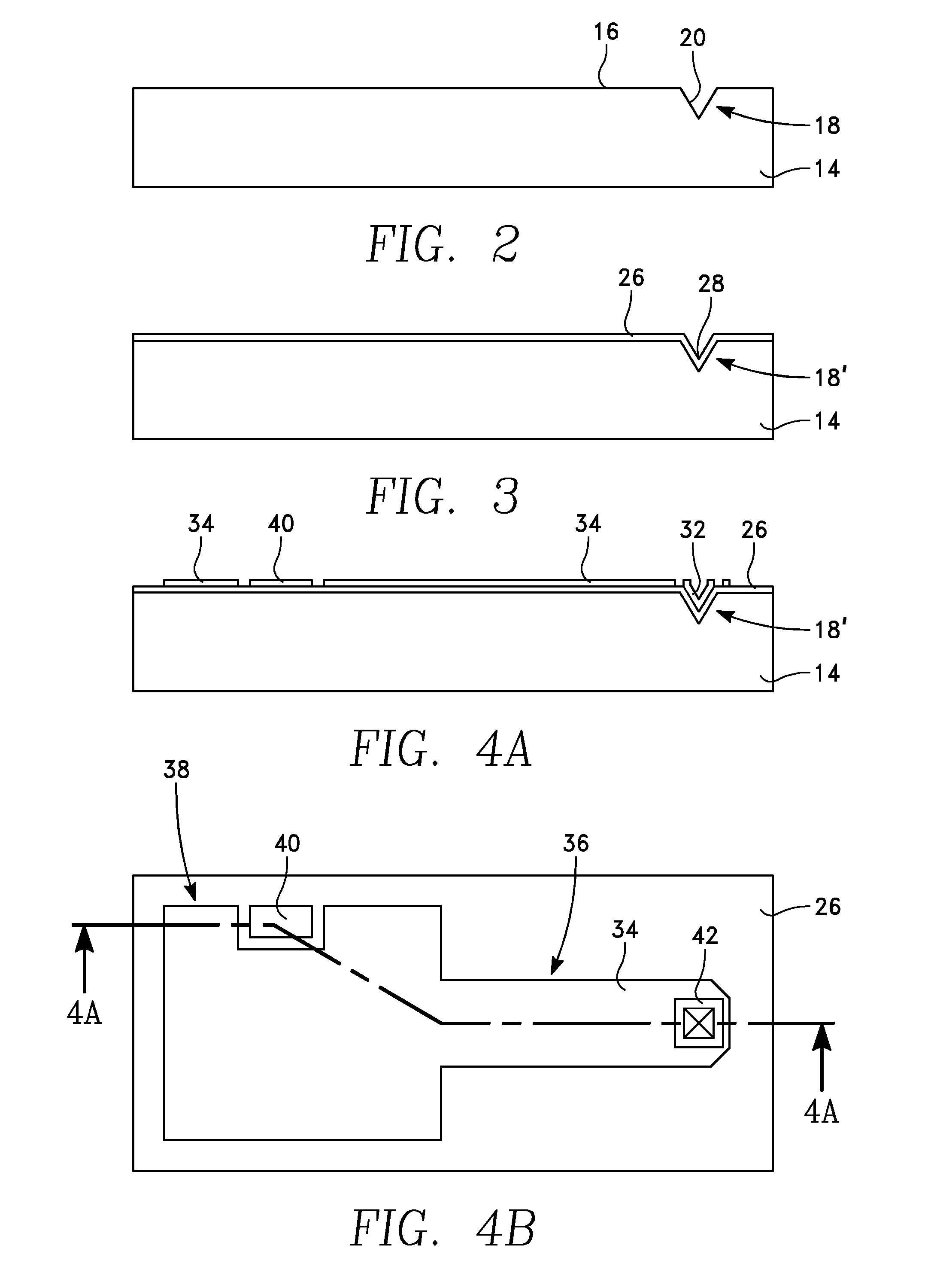
[0036]A first step 12 of this process processes a device wafer 14, as illustrated in the cross-sectional view of FIG. 2, of monocrystalline silicon ha...


PUM

PropertyMeasurementUnit
apex angleaaaaaaaaaa
frequencyaaaaaaaaaa
frequencyaaaaaaaaaa

Abstract

A microwave probe having a metal tip on the free end of a microcantilever. In one embodiment, a pyramidal pit is isotropically etched in a device wafer of monocrystalline silicon. Oxidation may sharpen the pit. Deposited metal forms the metal tip in the pit and a bottom shield. Other metal sandwiched between equally thick dielectric layers contact the tip and form a conduction path along the cantilever for the probe and detected signals. Further metal forms a top shield overlying the conduction path and the dielectrically isolated tip and having equal thickness to the bottom shield, thus producing together with the symmetric dielectric layers a balanced structure with reduced thermal bending. The device wafer is bonded to a handle wafer. The handle is formed and remaining silicon of the device wafer is removed to release the cantilever.

Description

FIELD OF THE INVENTION[0001]The invention relates generally to microwave microscopy. In particular, the invention relates to the structure and fabrication of a microwave probe and its sharp tip capable of imaging electrical characteristics of a sample on a microscopic scale.BACKGROUND ART[0002]Atomic force microscopy (AFM) has been extensively used to map the physical topography of samples on a sub-micron or even nanometer scale. In AFM, a nanometer-scale probe tip descends from a free end of a microcantilever. The tip is dragged or tapped along the surface of a sample and the deflection of the cantilever is measured to thereby determine the topography of the surface. Due to the simple structure of the tip, an AFM can measure only topographic properties of the sample, that is, its physical profile. Akamine et al. in seminal U.S. Pat. No. 4,943,719 has disclosed many ways to form an AFM probe.[0003]Microwave impedance microscopy has been developed based on many concepts of AFM in ord...

Claims


Application Information

Patent Timeline
Patent Type & Authority Patents(United States)
IPC IPC(8): G01Q60/38G01Q70/16
CPCB82Y20/00G01Q60/40G01Q60/22B82Y35/00
Inventor LI, XINXINYANG, YONGLIANG
Owner PRIMENANO
Why Eureka
Try Eureka