Non-destructive wafer-scale sub-surface ultrasonic microscopy employing near field AFM detection

a subsurface ultrasonic microscopy and wafer-scale technology, applied in the direction of instruments, mechanical roughness/irregularity measurements, specific gravity measurements, etc., can solve the problems of preventing the broad application of systems and methods, affecting the and no existing technique provides routine broad-adopted nanoscale sub-surface metrology routinely, etc., to achieve the effect of better resolution of the reconstruction step

Active Publication Date: 2012-12-04
BRUKER NANO INC
View PDF12 Cites 9 Cited by
  • Summary
  • Abstract
  • Description
  • Claims
  • Application Information

AI Technical Summary

Benefits of technology

[0016]In accordance with another aspect of the invention, the ultrasonic source may be driven into plural of harmonics, causing components with substantially higher frequency than the actuated frequency. High frequency components allow the diffraction limited resolution to be increased according to the harmonic frequency. Such harmonic components generally attenuate much faster than the base component, namely the first harmonics. A near field detection is desirable. Scanning probe detection in this invention should facilitate the near field detection.

Problems solved by technology

Despite broad demand from semiconductor, materials, and biomedical communities, no existing technique provides routine broadly adopted nanoscale sub-surface metrology.
Although systems exist for sub-surface metrology, each had limitations that prevent broad application of the systems and methods, as discussed in further detail below.
Existing techniques for performing sub-surface metrology are varied, although each is associated with particular limitations.
However, this technique requires destructive and time consuming thinning of samples, limiting its applicability.
However, the lateral resolution is limited by the wavelength of the ultrasonic excitation, typically in the range of millimeters to microns.
However, when applied at the nanoscale, these techniques are still destructive, requiring samples that are diced to less than 25 mm across and thinned to less than 100 um in thickness.
This technique provides contrast for materials with different thermal properties, but still suffers from optical resolution limits.
However, standard AFM imaging techniques are only sensitive to surface features or features a few nanometers below the surface.
Despite the above listed and described systems and the potential of SNFUH, the current state of the SNFUH technique makes it completely impractical for broad adoption in industry.
First, measurements have only been demonstrated on cm-scale samples, with areas more than 500× smaller than a conventional 300 mm silicon wafer.
There is currently no feasible technique to bond and debond ultrasonic actuators to meet these throughput requirements.
As such, current SNFUH techniques are not conveniently scalable to handle large samples.
Further, the semiconductor industry also places strict limits on backside particle contamination, a goal unlikely to be achieved with the current ultrasonic coupling requirements.
The cantilever, having a length of hundreds microns, can couple Mhz ultrasonic waves to the tip effectively but will fail to couple Ghz ultrasonic wave due to attenuation of the Ghz wave along the cantilever.

Method used


Image

  • Non-destructive wafer-scale sub-surface ultrasonic microscopy employing near field AFM detection
  • Non-destructive wafer-scale sub-surface ultrasonic microscopy employing near field AFM detection
  • Non-destructive wafer-scale sub-surface ultrasonic microscopy employing near field AFM detection

Examples


Embodiment Construction

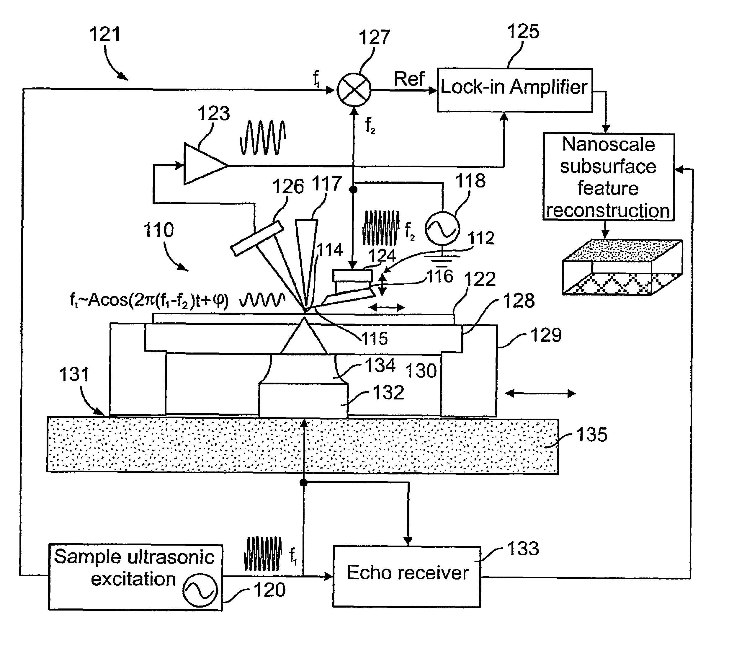
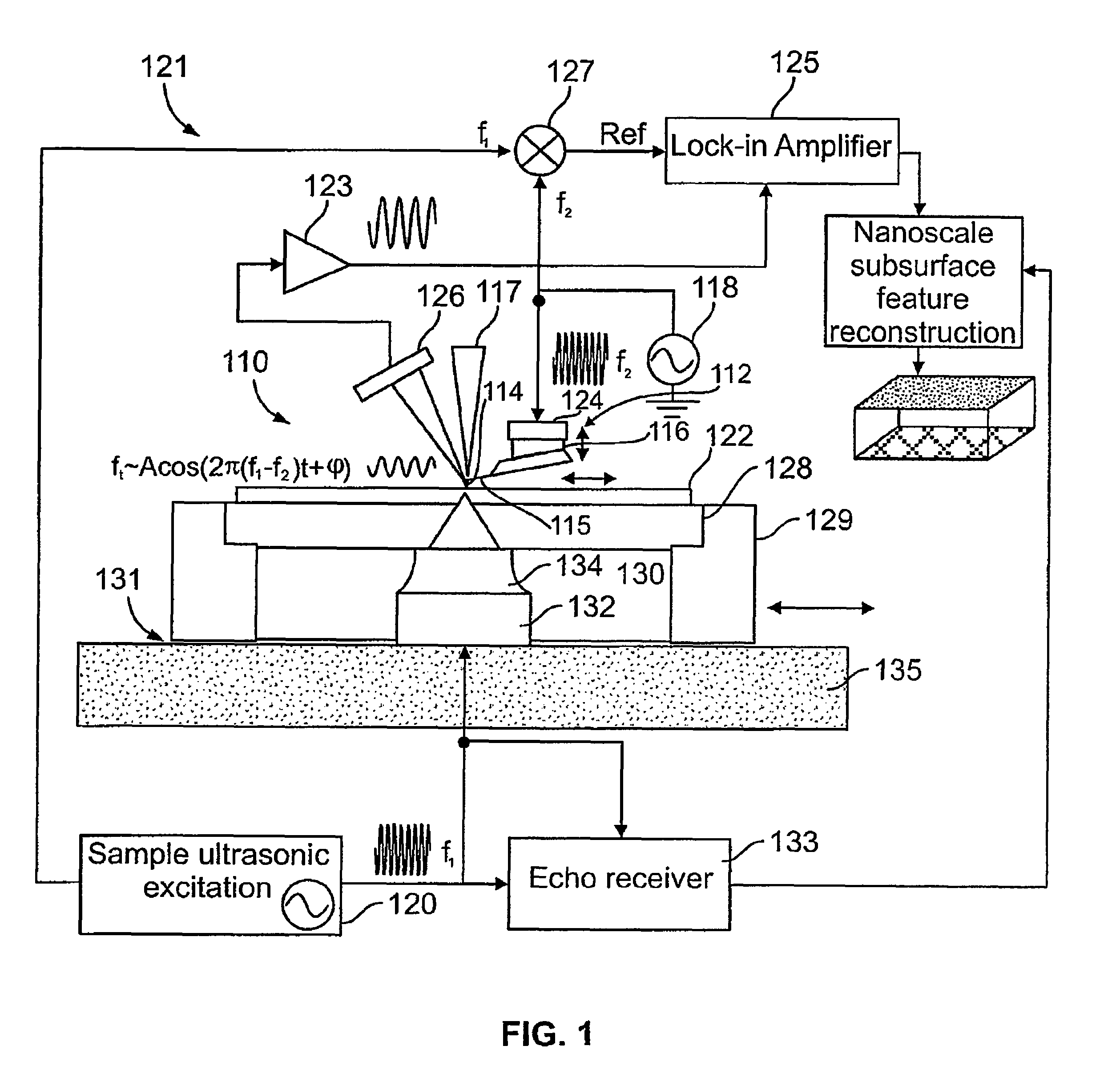
[0027]In a preferred embodiment of the invention, a scanning probe microscope (SPM) is used to obtain information about a sample through harmonic resonance imaging (HRI). The SPM may comprise any instrument that utilizes a tip-bearing probe to obtain information concerning a sample and that is capable of oscillating the tip. It may, for instance, comprise a scanning tunneling microscope (STM), a scanning magnetic force microscope (MFM), a scanning capacitance microscope (SCM), a scanning near-field optical microscope (NSOM), a scanning thermal microscope (SThM), or an atomic force microscope (AFM). An embodiment of the invention in the form of an AFM will now be disclosed, it being understood that the invention applies to all other SPMs as well.

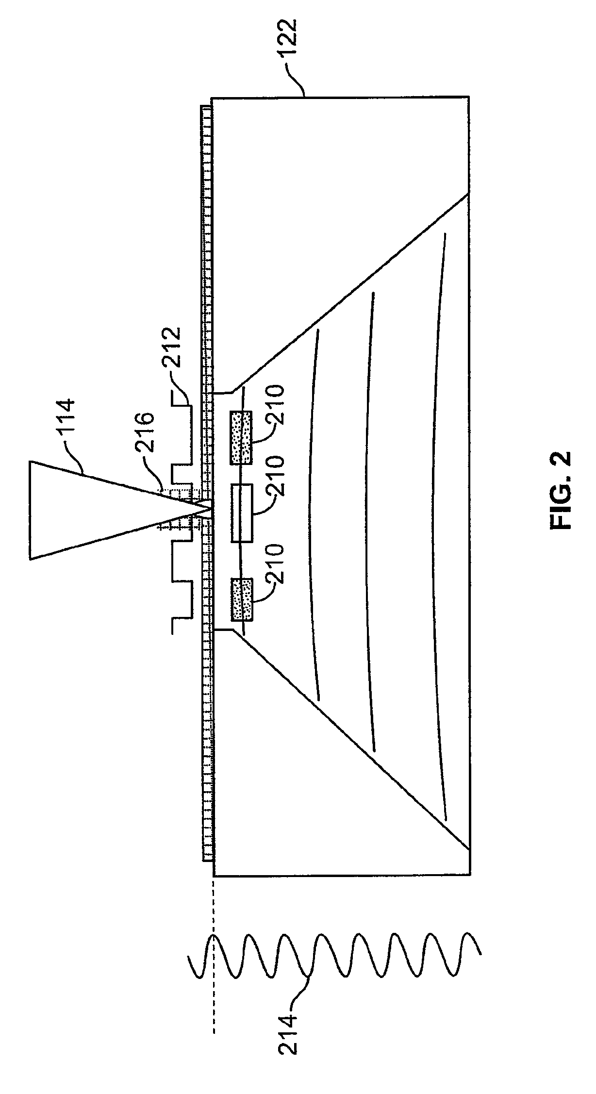
[0028]Referring now to FIG. 1, a schematic diagram of a nanoscale sub-surface metrology (NSM) instrument 100 is shown, according to an exemplary embodiment. A scanning probe microscope, such as an atomic force microscope (AFM) operates by pro...


PUM

PropertyMeasurementUnit
diameteraaaaaaaaaa
frequencyaaaaaaaaaa
thicknessaaaaaaaaaa

Abstract

A method, and corresponding apparatus, of imaging sub-surface features at a plurality of locations on a sample includes coupling an ultrasonic wave into a sample at a first lateral position. The method then measures the amplitude and phase of ultrasonic energy near the sample with a tip of an atomic force microscope. Next, the method couples an ultrasonic wave into a sample at a second lateral position and the measuring step is repeated for the second lateral position. Overall, the present system and methods achieve high resolution sub-surface mapping of a wide range of samples, including silicon wafers. It is notable that when imaging wafers, backside contamination is minimized.

Description

CROSS-REFERENCE TO RELATED APPLICATION[0001]This application claims the benefit of U.S. Provisional Application No. 60 / 917,307, filed May 10, 2007, incorporated herein by reference in its entirety.BACKGROUND OF THE INVENTION[0002]1. Field of the Invention[0003]The present application is directed to the field of metrology instruments and corresponding techniques, and more particularly to metrology tools capable of sub-surface imaging.[0004]2. Description of Related Art[0005]Despite broad demand from semiconductor, materials, and biomedical communities, no existing technique provides routine broadly adopted nanoscale sub-surface metrology. Surface metrology is the science of measuring small-scale features on surfaces. Surface primary form, surface waviness, and surface roughness are exemplary parameters that are measured. Sub-surface metrology is the study of parameters defining the constitution of a solid below the surface. One example of sub-surface metrology may include detecting s...

Claims


Application Information

Patent Timeline
Patent Type & Authority Patents(United States)
IPC IPC(8): G01N29/06
CPCB82Y35/00G01Q60/32G01Q60/06G01N29/0681B82Y20/00
Inventor PRATER, CRAIGSU, CHANMIN
Owner BRUKER NANO INC
Why Eureka
Try Eureka