Charged particle beam apparatus

a technology of chargeable particles and beams, which is applied in the direction of liquid/fluent solid measurement, machines/engines, instruments, etc., can solve the problems of increasing the cost of inspection systems, increasing the diameter of semiconductor devices, and increasing the structure and material of semiconductor devices, so as to reduce the cost of inspection, reduce the size of the installation space, and reduce the effect of cos

Inactive Publication Date: 2012-12-04
HITACHI HIGH-TECH CORP
View PDF7 Cites 0 Cited by
  • Summary
  • Abstract
  • Description
  • Claims
  • Application Information

AI Technical Summary

Benefits of technology

[0005]An object of the present invention is to provide a charged particle beam apparatus, which can be constructed with a smaller size (resulting in a small installation space) and a lower cost, suppress vibration, operate at higher speed, and be reliable in inspection. The charged particle beam apparatus is largely effective when a wafer having a large diameter is used.
[0007]As described above, the charged particle beam apparatus according to the present invention can be constructed with a smaller size (resulting in a small installation space) and a lower cost, suppress vibration, operate at higher speed, and be reliable in inspection. The charged particle beam apparatus is largely effective when a wafer having a large diameter is used.

Problems solved by technology

The structure and material of the semiconductor device have become increasingly complex.
On the other hand, there is a tendency that the diameter of a semiconductor device increases.
These affairs result in an increase in cost of an inspection system, reduction in the throughput of the device due to the increase in the size, and increase in risk of attachment of a foreign material to a wafer during transfer of the wafer in the complex inspection processes.
This causes reduction in reliability for the inspection which is the most important matter primarily.
This result in an increase in resistance required for driving each stage and an increase in residual vibration.
Therefore, as well as decreasing of accuracy of the inspection and increasing of the time period to move the stage, increase in the time period for evacuation leads to a reduction in the throughput of the device.
Installment of an inspection device having a large vacuum chamber in an expensive clean room may burden a user of the device with a large cost.

Method used


Image

  • Charged particle beam apparatus
  • Charged particle beam apparatus
  • Charged particle beam apparatus

Examples


Embodiment Construction

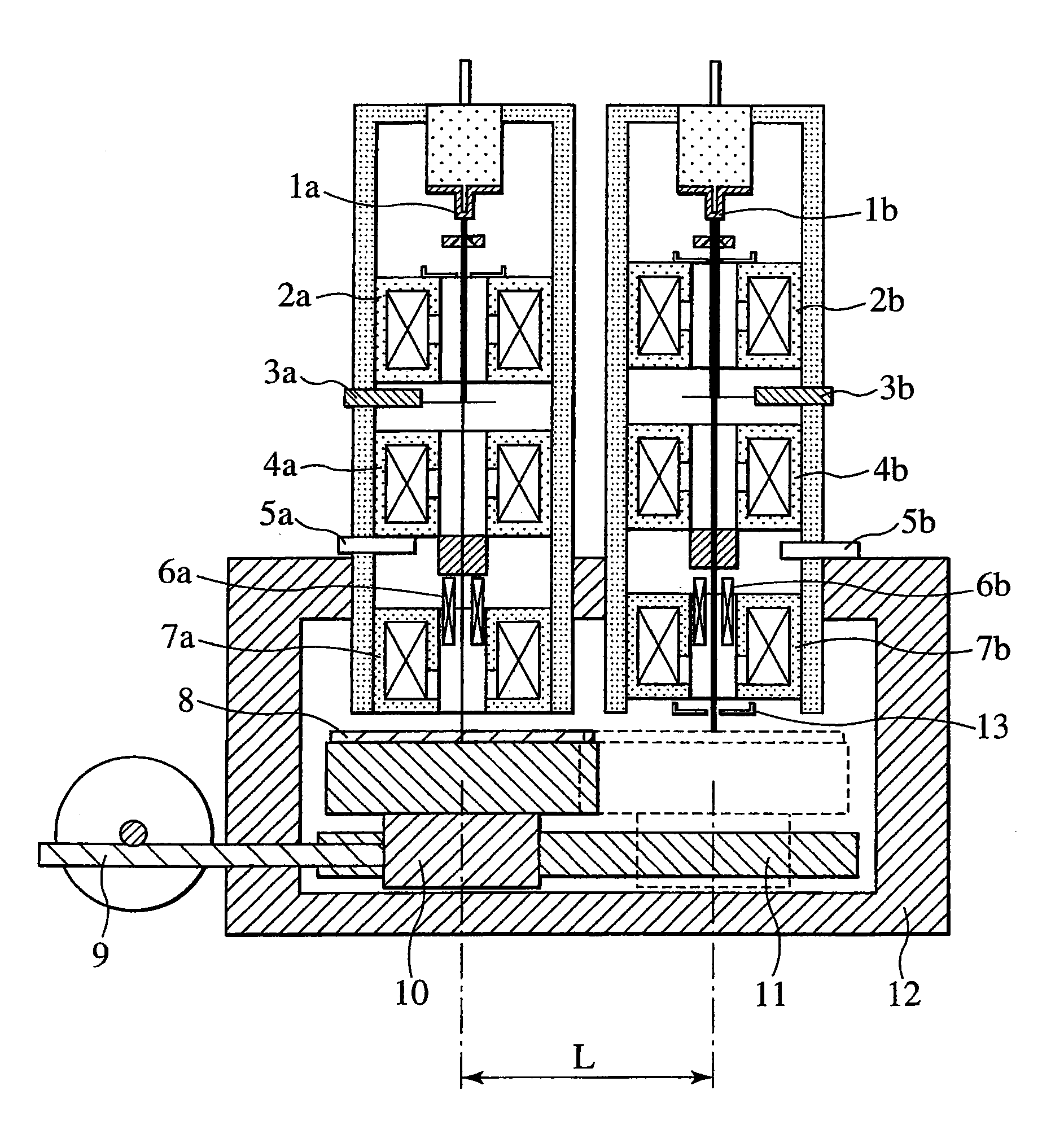
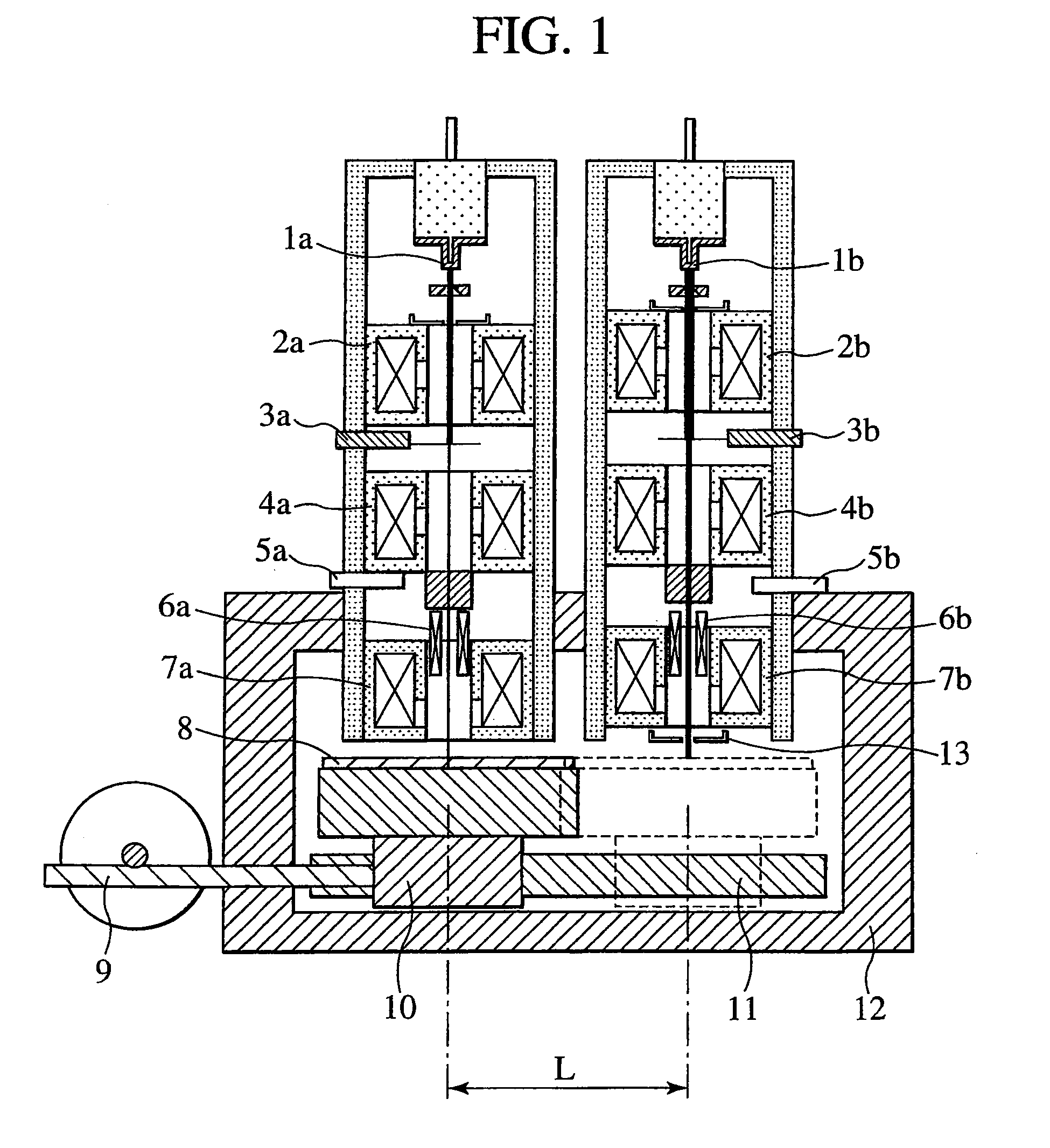
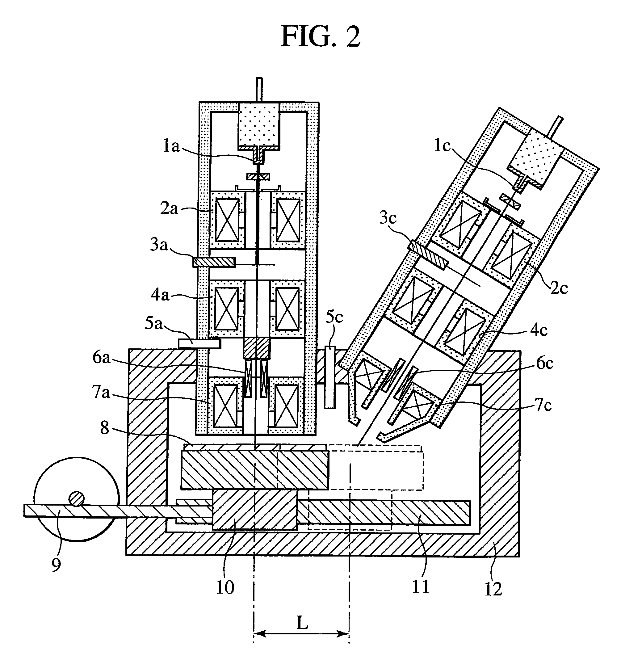
[0018]An embodiment of the present invention is described below. In order to accommodate to the increase in the diameter of a wafer and complex inspection processes, a plurality of inspection mechanisms are mounted on a single vacuum chamber, and a rotary stage and a single-shaft transfer mechanism are used to move a sample. That is, the single-shaft transfer mechanism is used to transfer the sample between the inspection mechanisms, and the rotary stage and a single-shaft transfer stage are used to position a target portion of the sample wafer. This configuration makes it possible to use the vacuum chamber having a size equal to or smaller than the half the size of a conventional XY transfer stage, suppress an increase in the weight of a movable part, and reduce the size of a charged particle beam apparatus according to the present embodiment compared with conventional techniques. This reduces a space to install the charged particle beam apparatus and a cost of the device, compared...


PUM


Abstract

A charged particle beam apparatus can be constructed with a smaller size (resulting in a small installation space) and a lower cost, suppress vibration, operate at higher speed, and be reliable in inspection. The charged particle beam apparatus is largely effective when a wafer having a large diameter is used. The charged particle beam apparatus includes: a plurality of inspection mechanisms, each of which is mounted on a vacuum chamber and has a charged particle beam mechanism for performing at least an inspection on the sample; a single-shaft transfer mechanism that moves the sample between the inspection mechanisms in the direction of an axis of the single-shaft transfer mechanism; and a rotary stage that mounts the sample thereon and has a rotational axis on the single-shaft transfer mechanism. The single-shaft transfer mechanism moves the sample between the inspection mechanisms in order that the sample is placed under any of the inspection mechanisms. The rotary stage positions the sample such that a target portion of the sample can be inspected by the inspection mechanism under which the sample is placed, and the inspection mechanisms inspect the sample.

Description

BACKGROUND OF THE INVENTION[0001]1. Field of the Invention[0002]The present invention relates to a charged particle beam apparatus that uses a charged particle beam such as an electron beam and an ion beam to observe and process a sample.[0003]2. Description of the Related Art[0004]In objects observed by a charged particle beam apparatus, a semiconductor device has a circuit pattern which has been miniaturized. Therefore, in addition to increase the sensitivity of an optical system, methods for inspecting and processing a semiconductor wafer by using a charged particle beam have attracted attention. An inspection device using a scanning electron microscope (SEM) has been developed. In order to inspect a semiconductor wafer on which a semiconductor device is formed, a defect review SEM and a critical dimension SEM are used. The defect review SEM is designed to use an optical image or an image obtained by scanning using a charged particle beam, detect a defect based on the image, and ...

Claims


Application Information

Patent Timeline
Patent Type & Authority Patents(United States)
IPC IPC(8): G01F23/00G21K5/10G21K5/08
CPCH01J37/20H01J37/28H01J37/30H01J2237/0216H01J2237/20214H01J2237/20221
Inventor ITO, HIROYUKISASAKI, YUKOOTAKA, TADASHI
Owner HITACHI HIGH-TECH CORP
Why Eureka
Try Eureka