Receiver apparatus and reception method

a receiver and receiver technology, applied in the field of digital wireless receivers, can solve the problems of difficult to handle a complex modulated signal, risk of oscillation, and the filter may become an unstable filter, so as to reduce the chip area and power consumption of the receiver apparatus, reduce the waste of excessive flow, and achieve large-capacity communication.

Active Publication Date: 2013-01-01
NEC CORP
View PDF8 Cites 0 Cited by
  • Summary
  • Abstract
  • Description
  • Claims
  • Application Information

AI Technical Summary

Benefits of technology

[0056]First, the digital RF technology in Patent Document 2 described above can accommodate reduced power consumption and lower cost. However, it is difficult for the digital RF technology in Patent Document 2 to handle a complicated modulated signal such as multi-ary data (m-ary data, where m>=2).
[0101]The present invention can realize a radio receiver apparatus with a high data rate. The present invention allows a large-capacity OFDM communication technology characterized by low power and area saving in the weak radio frequency band, for example. Reception and transmission of data of an amount comparable to wireless LAN can be performed in a use of a sensor net as well. Further, the present invention allows completion of data reception and transmission in a short time. Thus, it is enough to achieve moderate Tx−Rx synchronization, which leads to cost reduction of the overall system.

Problems solved by technology

In the case of the offset quadrature phase shift keying, however, the data transition of the 180-degree phase shift is not allowed and thus there remains two types of phase transition patterns comprised of ±90 degrees phase shifts.
The filter may thereby become an unstable filter accompanied by a risk of oscillation.
First, the digital RF technology in Patent Document 2 described above can accommodate reduced power consumption and lower cost. However, it is difficult for the digital RF technology in Patent Document 2 to handle a complicated modulated signal such as multi-ary data (m-ary data, where m>=2).
The reason for that difficulty is that, since demodulation is performed by reading the instantaneous time waveform of the modulated signal, it is difficult to instantaneously read the multi-ary data whose time waveform becomes complicated on a time axis.
However, it is difficult to achieve reduced power consumption and lower cost.
These requirements mean an increase in power and area overhead.
However, in an application such as sensor net communication, which severely requires low power operation and low cost, it is difficult to use these ADC and DSP with a large overhead.
This has become a factor of hampering use of the large-capacity OFDM communication in a weak radio frequency band.

Method used


Image

  • Receiver apparatus and reception method
  • Receiver apparatus and reception method
  • Receiver apparatus and reception method

Examples


Embodiment Construction

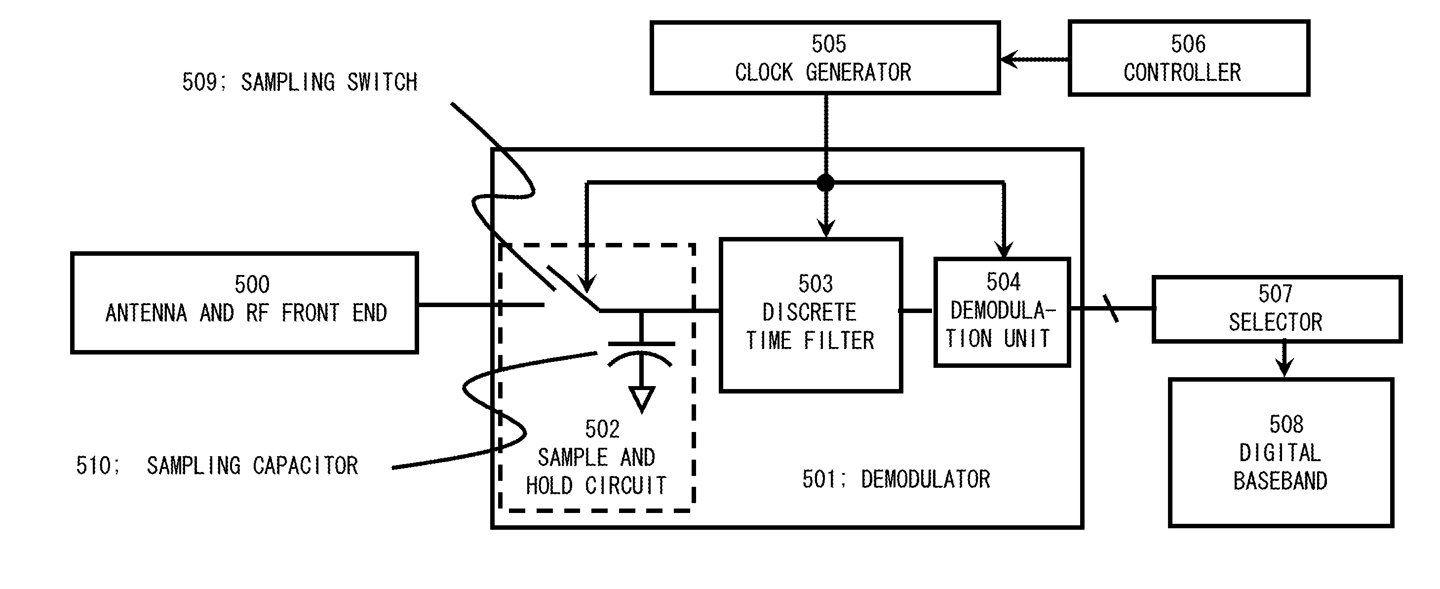
[0111]Exemplary embodiments of the present invention will be described. A digital radio receiver according to the present invention includes a sampler circuit (502), a demodulator (504), and a discrete time filter (503). The sampler circuit (502) receives and samples an FDM (Frequency Division Multiplexing) signal obtained by multiplexing a plurality of subcarriers f1, f2, . . . and fN on a frequency axis to perform sampling in order to increase the number of data per symbol with respect to a 2-ary (binary) modulation (BPSK, BFSK) using a single carrier wave that has been used in a weak radio frequency band. The demodulator (504) completes demodulation of a particular subcarrier f1 for the FDM signal within a short period of time (within one symbol data period), and then switches a frequency for the demodulator to a frequency for the different subcarrier f2, and completes demodulation of the subcarrier f2 within the short period of time, as in the case of the subcarrier f1. The disc...


PUM


Abstract

A receiver includes a sample and hold circuit that receives a signal (continuous time signal) that has been subject to frequency division multiplexing modulation, converts the signal to a discrete time signal, and outputs the discrete time signal, a discrete time filter that receives the signal output from the sample and hold circuit and attenuates a frequency component of a subcarrier different from a specified subcarrier, and a demodulation unit that extracts a digital baseband from a signal that has passed through the discrete time filter to complete a demodulation operation within one data symbol reception period.

Description

[0001]This application is the National Phase of PCT / JP2008 / 066631, filed on Sep. 16, 2008, which is based upon and claims the benefit of the priority of Japanese patent application No. 2007-243939 filed on Sep. 20, 2007, the disclosure of which is incorporated herein in its entirety by reference thereto.TECHNICAL FIELD[0002]The present invention relates to a digital wireless receiver. More specifically, the invention relates to a receiver of a signal which has been subject to frequency division multiplexing and has been then transmitted.BACKGROUND ART[0003]The reduction of thermal noise and increase in operation speed that have been accomplished by the miniaturization of CMOS (Complementary MOS) technology have made it possible for a radio communication front-end circuit to be formed of CMOS. The radio communication front-end circuit has been hitherto formed of a compound semiconductor such as gallium arsenide, silicon germanium or the like, or silicon bipolar device.[0004]In recent...

Claims


Application Information

Patent Timeline
Patent Type & Authority Patents(United States)
IPC IPC(8): H03K9/00
CPCH04B1/0007H04B1/28H04L27/2649H04L27/26524
Inventor ISHIZAKI, HARUYA
Owner NEC CORP
Why Eureka
Try Eureka