
Method for transferring a nanolayer

a nanolayer and nanotechnology, applied in the field of nanolayer transfer, can solve the problems of not enabling a controlled transfer onto another substrate, all these layers can only obtain a technical relevance,

Active Publication Date: 2013-02-19
CNM TECH
View PDF19 Cites 15 Cited by
  • Summary
  • Abstract
  • Description
  • Claims
  • Application Information

AI Technical Summary

Benefits of technology

The present invention describes a method for handling a nno-layer, which involves using a transfer medium that is transformed from a liquid or gas to a solid phase. The transfer medium is applied to a first substrate, separated from the nano-layer, and then transferred to a second substrate. The transfer medium is dissolved or removed in a further process step. This method is particularly useful for manufacturing substrates for transmission electron microscopy, where the nano-layer is arranged on a TEM grid. The technical effects of this patent include improved stability and versatility in handling the nano-layer and the ability to easily manufacture substrates for transmission electron microscopy.

Problems solved by technology

However, all of these layers can only obtain a technical relevance if it succeeds to make them in a simple manner manipulable, i.e. to transfer the layer essentially non-destructively from one support (substrate) to another support.
However, this still does not enable a controlled transfer onto another substrate.

Method used


Image

  • Method for transferring a nanolayer
  • Method for transferring a nanolayer
  • Method for transferring a nanolayer

Examples


example 1

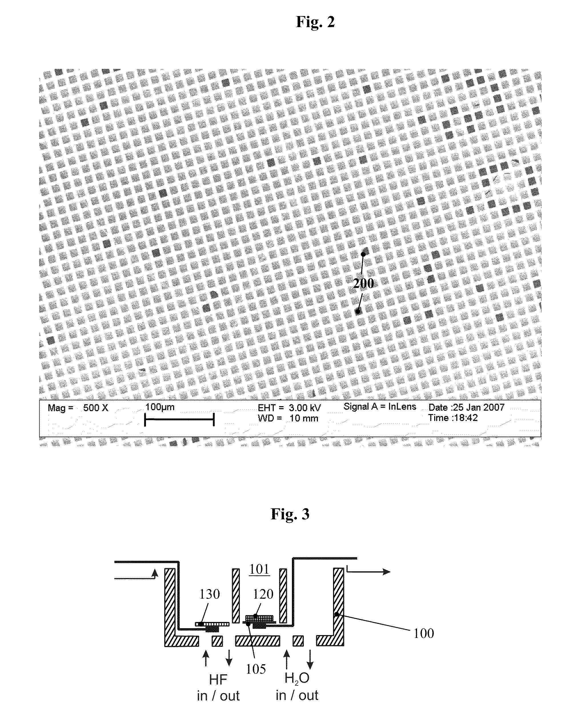
[0028]Transfer of a cross-linked monolayer of 4′-[(3-trimethoxysilyl) proproxy]-[1,1′-biphenyl]-4-carbonitril (in the following monolayer (I)) to a TEM grid. Such a monolayer has significant advantages for electron microscopy. The layer thickness is given by the length of the monomers from which the monolayer is formed. Therefore, it is to a large extent homogenous and is approximately 1.5 nm. Compared to this, conventional TEM substrates are significantly thicker leading to a less sample contrast in the TEM image. Chemical nano-lithography can be executed on the monolayer (I), cf. Biebricher A. et al.; Journal of Biotechnology 112, 97, (2004). With it, for example organic molecules can be bound on well defined positions onto the monolayer (I).

[0029]For the manufacture of the coated TEM grid the monolayer (I) is at first prepared on a silicon substrate coated with silicon nitride. The silicon is used in this example as carrier substrate; the silicon nitride layer serves as a sacrifi...

example 2

Transfer of a Structured Monolayer (I) to a Gold Substrate

[0036]Nano-layers with self-aggregating monolayers (SAM) can be prepared on a number of substrates. For this purpose, a suitable SAM substrate combination has to be known. For example, the monolayer can be used as resist for wet chemical etching or for metal deposition. Furthermore, (bio-)molecules can be coupled by “chemical lithography”.

[0037]However, for a given substrate a suitable molecule is not always available to generate monolayers. In particular, a lot of effort is necessary to obtain a new SAM substrate combination and to characterize it. For lithographical processes it is in addition generally necessary that the substrate is plain.

[0038]With the inventive transfer of monolayers it is however possible to use known SAM substrate combinations the previous lithographical structuring can be made on a flat substrate. The transfer can then occur to curved surfaces as well as on substrates on which no SAM can be formed.

[0...

example 3

Transfer of a 1,1′-biphenyl-4-thiol monolayer (in the following monolayer (II)) to a silicon oxide substrate

[0041]In this example, the monolayer (II) is at first prepared on mica coated with gold. The mica serves as carrier substrate, the gold serves as sacrificial layer and the monolayer (II) is the monolayer to be transferred. As transfer medium a photoresists is used (for example AR-P 3510 of Allresist GmbH, www.allresist.de). The resist is spun onto the carrier substrate and hardened on a heating plate.

[0042]In the next step, the mica substrate is striped layer by layer with a tape (for example Scotch tape of 3M); alternatively it can be dissolved in hydrofluoric acid. Afterwards, the gold (sacrificial layer) is removed (for example with an iodine / potassium iodine solution or potassium cyanide solution) by allowing the sample to float on the etching solution. With a tweezers a silicon oxide sample can now be dipped into the solution, and thus the monolayer (II) with the photores...


PUM

PropertyMeasurementUnit
thicknessaaaaaaaaaa
dissolvingaaaaaaaaaa
transmission electron microscopyaaaaaaaaaa

Abstract

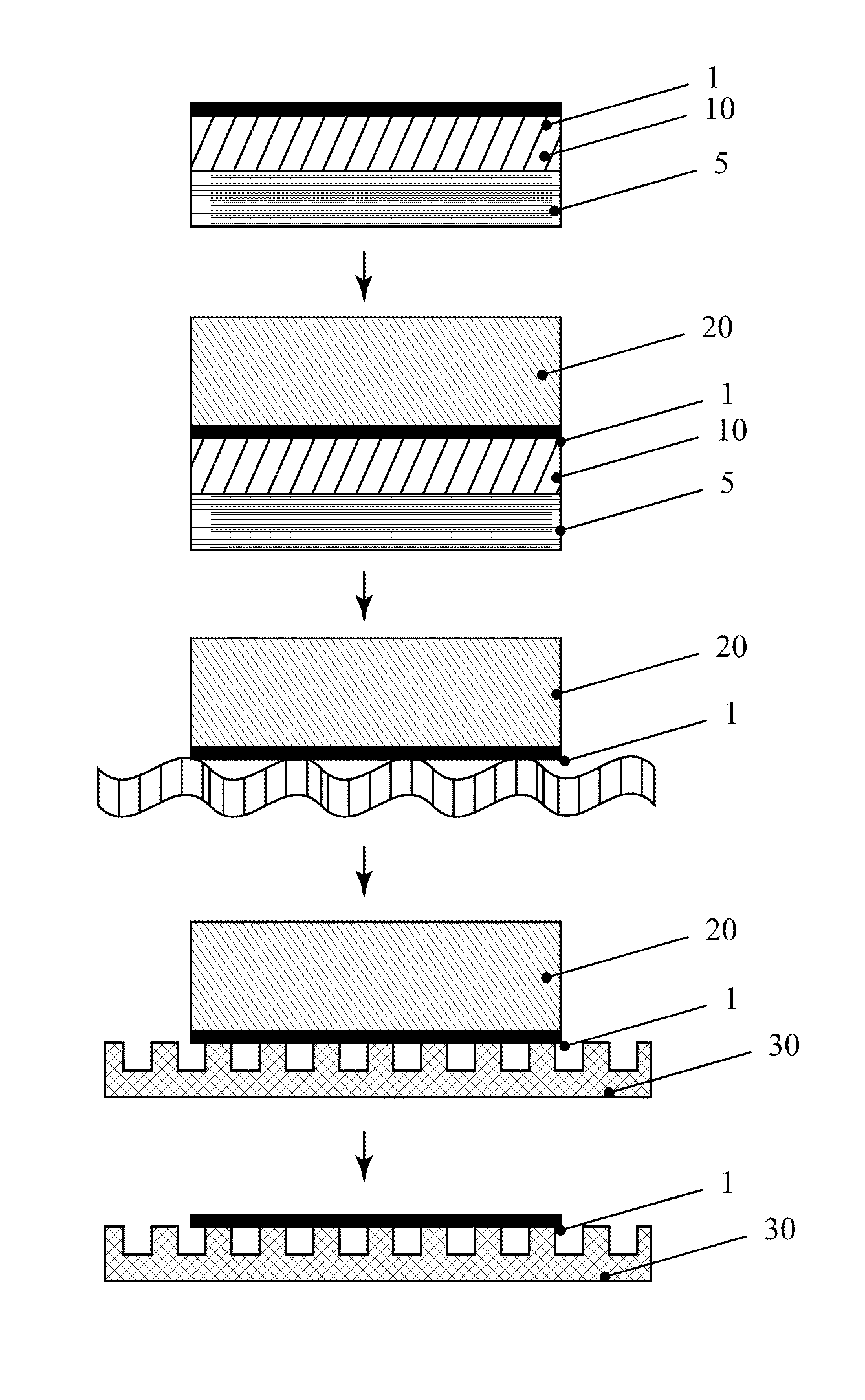
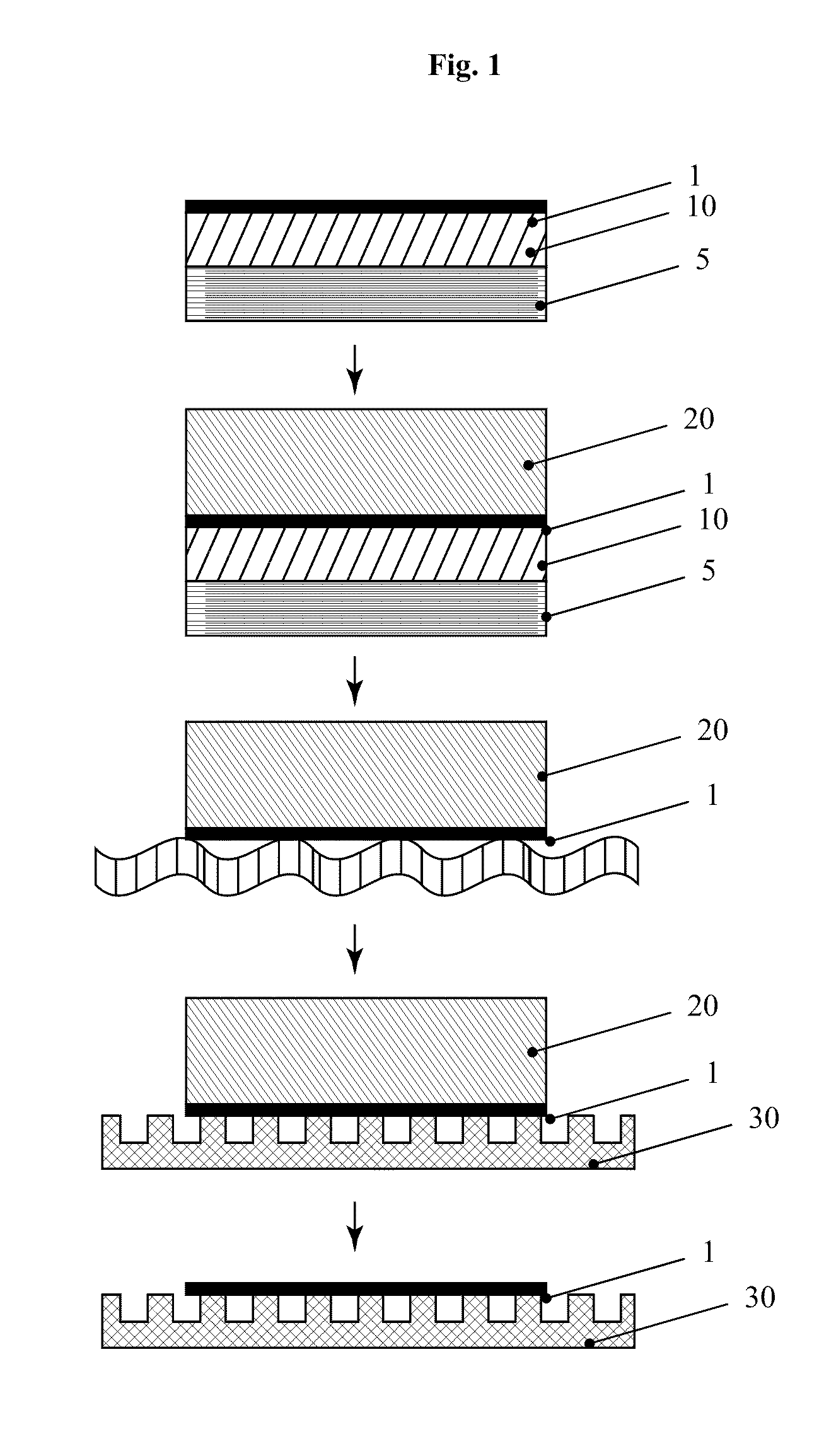
The invention relates to a method for transferring a nano-layer (1) from a first substrate (5, 105) to a second substrate (30, 130), wherein the nano-layer (1) comprises a self-aggregating monolayer with cross-linked phenyl units and / or a mono-atomic graphite layer (graphene), wherein the method comprises the following steps:a. applying a transfer medium (20, 120) onto nano-layer (1), wherein in this step or afterwards the transfer medium (20, 120) is transformed from a liquid or gaseous phase in a solid phase;b. separating the transfer medium (20, 120) and the nano-layer (1) from the first substrate (5, 105); andc. applying the transfer medium (20, 120) and the nano-layer (1) onto the second substrate (30, 130); andd. removing the transfer medium (20, 120).

Description

1. TECHNICAL FIELD[0001]The invention relates to a method for transferring a nano-layer from a first substrate to a second substrate as well as a transmission electron microscopy (TEM) substrate covered with a nano-layer using this method.2. PRIOR ART[0002]The manufacturing and the application of objects with dimensions in the nanometer range are the objectives of nano-technology. For example nano-spheres, nano-wires or also so called “nano-tubes” made of carbon are known. Nano-tubes are an example that objects of the nano-technology can have in one dimension absolutely macroscopic dimensions, while their extents in one or several other directions are limited to the nanometer range.[0003]Nano-layers are a further technically important example. In the following this shall mean a layer of any material having in two directions macroscopic dimensions, i.e. in the micrometer range or above, while the thickness of the layer is limited to at most 10 nm. In doing so, the nano-layer has not ...

Claims


Application Information

Patent Timeline
Patent Type & Authority Patents(United States)
IPC IPC(8): B32B37/14B32B38/10B32B43/00
CPCB05D1/283B81C1/0038B82Y30/00B82Y40/00B81C2201/0191
Inventor GOLZHAUSER, ARMINNOTTBOHM, CHRISTOPHBEYER, ANDRE
Owner CNM TECH
Learn More