
High efficiency module

a module and high-efficiency technology, applied in the field of modules, can solve the problems of electromagnetic interference (emi), deterioration of the switching performance increase in power consumption of the dc-dc converter, etc., and achieve the effect of reducing the wiring inductance and reducing the wiring resistan

Active Publication Date: 2013-03-05
ROHM CO LTD
View PDF8 Cites 22 Cited by
  • Summary
  • Abstract
  • Description
  • Claims
  • Application Information

AI Technical Summary

Benefits of technology

[0009]The present invention has been proposed under the foregoing circumstances. An object of the present invention is to provide a module with reduced wiring resistance and reduced wiring inductance.
[0012]The above arrangement contributes to reducing the wing resistance and inductance between the functional devices, compared with an instance where the first functional device and the second functional device are connected through an interconnection line formed on a printed circuit board. Accordingly, a circuit including such a module can achieve lower power consumption and higher performance. In addition, the portion of the frame serving as the connection terminal can be used for making a connection to another device on the circuit, which allows the user a higher degree of freedom in designing the circuit.
[0014]Also in the above case, where the two functional devices are both transistors, it is possible to reduce the wiring resistance and inductance between the electrodes directly connected to the frame.
[0016]Such configuration minimizes the distance between the electrodes directly connected to the frame, thereby further reducing the wiring resistance and inductance.
[0018]Such configuration enables reduction in wiring resistance and inductance between the collector electrode of the first functional device and the emitter electrode of the second functional device.

Problems solved by technology

The wiring resistance leads to an increase in power consumption of the DC-DC converter 100, and the wiring inductance leads to deterioration of switching performance of the DC-DC converter 100.
In addition, the wiring inductance may cause electromagnetic interference (EMI).
Specifically, the wiring inductance generates a magnetic field, and when the magnetic field fluctuates, noise is generated in the circuit.
Such noise degrades the performance of the DC-DC converter 100.
This makes the foregoing issue more serious.

Method used


Image

  • High efficiency module
  • High efficiency module
  • High efficiency module

Examples


first embodiment

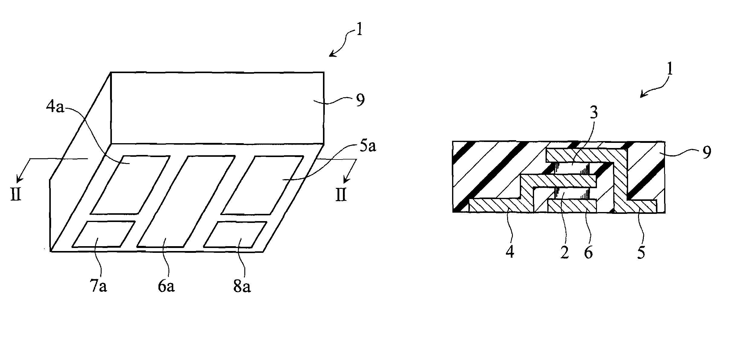
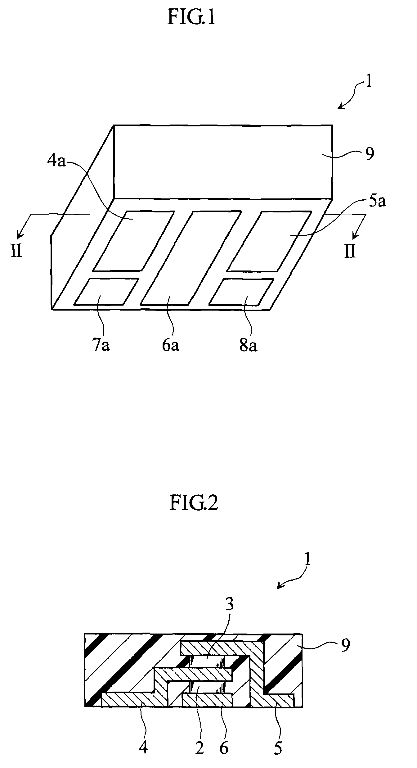
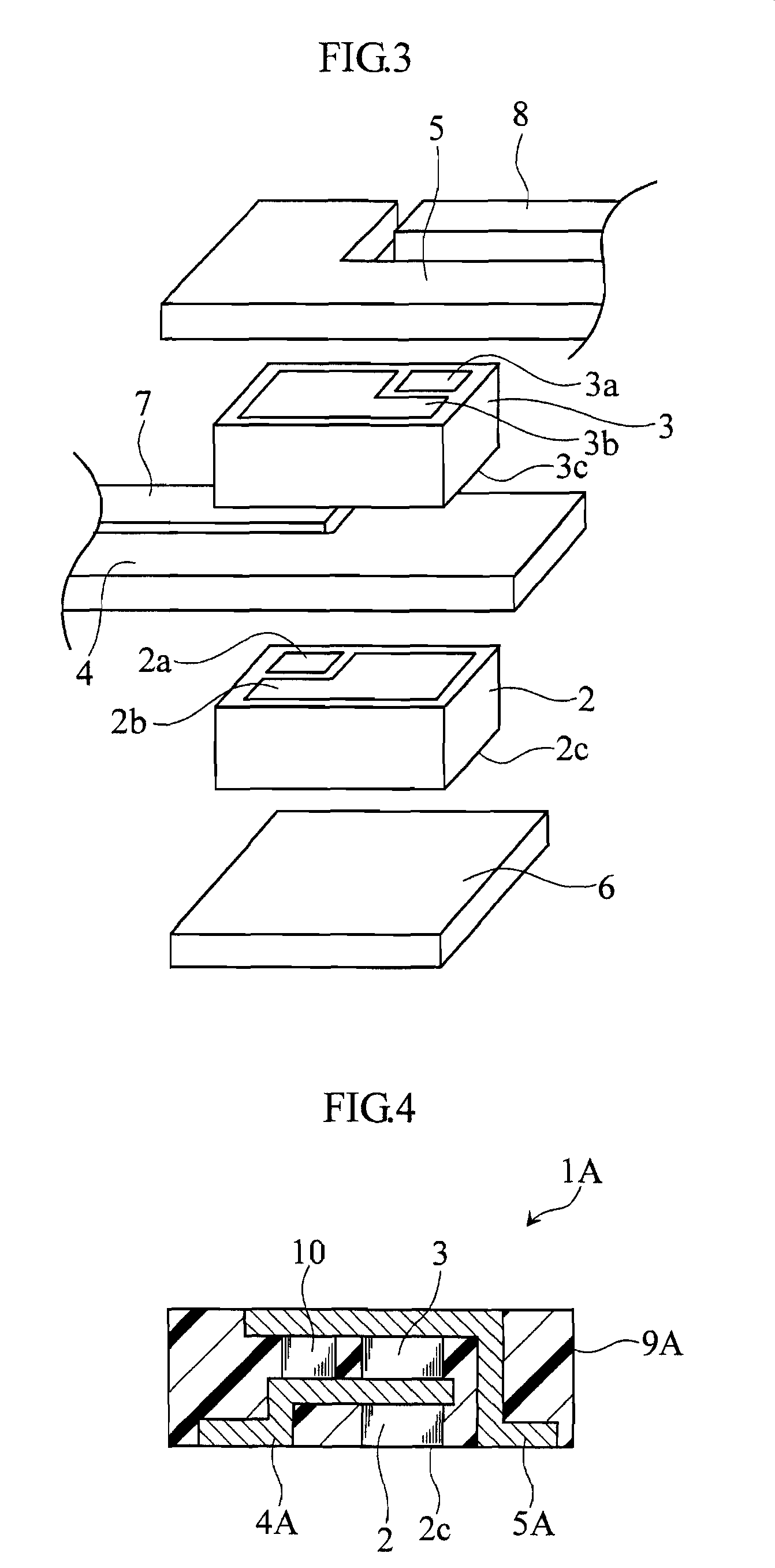
[0034]Embodiments of the present invention will be described below with reference to the accompanying drawings. FIGS. 1 to 3 illustrate a module according to the present invention. The module of this embodiment corresponds to a single device into which the high-side MOSFET 110 and the low-side MOSFET 120 shown in FIG. 13 are integrated.

[0035]The illustrated module 1 includes a high-side MOSFET chip 2, a low-side MOSFET chip 3, conductive lead frames 4-8, and a resin package 9.

[0036]As shown in FIG. 3, the upper surface of the high-side MOSFET chip 2 is provided with a gate electrode 2a and a source electrode 2b, and the lower surface of the chip is provided with a drain electrode 2c. As known, a bipolar transistor has three electrodes called a base electrode, an emitter electrode, and a collector electrode. These electrodes correspond to the gate electrode, the source electrode, and the drain electrode of a MOSFET, respectively.

[0037]The gate electrode 2a of the high-side MOSFET chi...

fourth embodiment

[0064]By using the module 1C of the fourth embodiment for the MOSFET 21 and the diode 22 of the step down DC-DC converter 20 shown in FIG. 11 (indicated by dotted lines in FIG. 11), the wiring resistance and inductance between the source electrode of the MOSFET 21 and the cathode electrode of the diode 22 can be reduced. This enables reduction in power consumption and improvement in performance of the step down DC-DC converter 20.

[0065]A module according to the fifth embodiment of the present invention differs from the module 1 of the first embodiment (see FIG. 2) in that an NPN transistor and a PNP transistor are employed in place of the high-side MOSFET chip 2 and the low-side MOSFET chip 3, respectively. Drawings to illustrate the fifth embodiment are omitted since they would be the same as FIGS. 1-3.

[0066]FIG. 12 is a circuit diagram of a drive circuit. A drive circuit 30 includes an NPN transistor 31, a PNP transistor 32, capacitors 33, 34, a gate resistance 35, a resistance 36...

fifth embodiment

[0068]By using the module of the fifth embodiment for the NPN transistor 31 and the PNP transistor 32 of the drive circuit 30 shown in FIG. 12 (indicated by bold dotted lines in FIG. 12), the wiring resistance and inductance between the emitter electrode of the NPN transistor 31 and the emitter electrode of the PNP transistor 32 can be reduced. This enables reduction in power consumption and improvement in performance of the drive circuit 30.


PUM


Abstract

A module (1) includes a first functional device (2) and a second functional device (3). The first functional device (2) includes a base electrode, an emitter electrode and a collector electrode. The second functional device (3) includes at least one electrode. The module (1) further includes a conductive frame (4). One of the base electrode, the emitter electrode, and the collector electrode of the first functional device (2) is directly connected to the frame (4). The electrode of the second functional device (3) is also directly connected to the frame (4). The frame (4) includes a portion serving as a terminal for external connection.

Description

TECHNICAL FIELD[0001]The present invention relates to a module with reduced wiring inductance and resistance between mutually connected functional devices.BACKGROUND ART[0002]A synchronous rectification type DC-DC converter that includes a metal oxide semiconductor field effect transistor (MOSFET) in place of a rectifying diode is known. FIG. 13 is a schematic diagram showing the configuration of a synchronous rectification type DC-DC converter. The illustrated DC-DC converter 100 includes a high-side MOSFET 110, a low-side MOSFET 120, a Schottky barrier diode (SBD) 130, a coil 140, a capacitor 150, and a control IC 160. The DC-DC converter 100 is controlled by the control IC 160 so as to alternately supply current to the high-side MOSFET 110 and the low-side MOSFET 120, to reduce the voltage.[0003]The conventional DC-DC converter 100 is made by mounting the foregoing functional devices on a printed circuit board, and then electrically connecting the electrodes of each functional de...

Claims


Application Information

Patent Timeline
Patent Type & Authority Patents(United States)
IPC IPC(8): H01L29/76H01L21/00H01R9/00
CPCH01L23/3107H01L23/49551H01L24/33H01L25/117H01L23/49562H01L23/49575H01L24/41H05K7/14H01L2924/1305H01L2924/12032H01L2924/1306H01L2224/33181H01L2224/32245H01L24/29H01L2924/01029H01L2924/01082H01L2924/014H01L2924/0781H01L2924/13055H01L2924/13091H01L2924/19041H01L2924/30107H01L2924/01006H01L2924/01033H01L2924/00H01L2924/181H01L2224/40245H01L24/40H01L2224/84801H01L2224/83801H01L2924/00014H01L2224/8485H01L2224/0603H01L24/84H01L2924/00012H01L2224/37099H01L23/49537H01L24/39H01L24/36H01L23/49513H01L24/30H01L24/37H01L25/072H01L25/074H01L23/49555H01L29/78H01L23/4951H01L23/49805
Inventor YOSHIMOCHI, KENICHI
Owner ROHM CO LTD
Learn More