Wireless IC device

a technology of ic chip and wireless IC, which is applied in the direction of burglar alarm mechanical actuation, protective material radiating elements, instruments, etc., can solve the problems of undesirable damage to the ic chip and narrow usable frequency band of the wireless ic device, and achieve the effect of small frequency-characteristic varian

Inactive Publication Date: 2013-03-05
MURATA MFG CO LTD
View PDF324 Cites 2 Cited by
  • Summary
  • Abstract
  • Description
  • Claims
  • Application Information

AI Technical Summary

Benefits of technology

[0010]Since impedance of the wireless IC chip and the radiation plate is matched by adjusting inductance of the linear electrode and capacitance generated between the planar electrode and the linear electrode in the wireless IC device according to a preferred embodiment of the present invention, capacitance variance decreases, as a result of which frequency-characteristic variance reduces. When the linear electrode includes a plurality of loops, capacitance between lines of the linear electrode is also used in impedance matching. Furthermore, by setting different line lengths for the plurality of neighboring electrodes, a resonance frequency can be appropriately set for each linear electrode and a wide-band gain characteristic can be obtained.
[0011]In the wireless IC device according to a preferred embodiment of the present invention, an end portion of the linear electrode may be arranged to face the planar electrode and may be coupled to the planar electrode through an electric field. Since the wireless IC chip and the radiation plate are not electrically connected directly, static electricity from the radiation plate is not applied to the wireless IC chip and, thus, it is possible to prevent the statistic electricity from damaging the wireless IC chip. Furthermore, a large capacitance value can be set for capacitance generated between the planar electrode and the end portion of the linear electrode and capacitance variance due to variance in a gap between lines of the linear electrode can be decreased, which thus reduces variance in a usable frequency.
[0012]In addition, the planar electrodes may be arranged on different principal surfaces of the feeder circuit board so as to face each other. By arranging the planar electrodes on the respective principal surfaces of the substrate, capacitance using the substrate as a dielectric can be formed between the planar electrodes. By combining this capacitance with capacitance between the feeder circuit board and the radiation plate, fine adjustment of the capacitance value becomes easier and the resonance-frequency variance and the impedance variance can be reduced.
[0013]Additionally, the linear electrode and the radiation plate may be arranged symmetrically with respect to the wireless IC chip. With this configuration, a radiation characteristic of the left and right radiation plates can be made equal and designing of impedance matching becomes easier.
[0014]An insulating film may be arranged on the feeder circuit board so as to cover at least the planar electrode. Alternatively, an insulating film may be arranged on a substrate having the radiation plate located thereon so as to cover the radiation plate. Since the planar electrode and the radiation plate are protected by the insulating film, environmental resistance (particularly, a rust prevention effect) improves. Furthermore, the feeder circuit board or the radiation plate can be individually sold in the market.

Problems solved by technology

However, since matching is performed in the wireless IC device only in a frequency determined by the inductance of the matching units and the capacitance generated between the main antenna elements and the auxiliary antenna element, the wireless IC device undesirably has a narrow usable frequency band.
Furthermore, since the IC chip and the main antenna elements are electrically connected, static electricity from the main antenna elements is applied directly to the IC chip, which undesirably damages the IC chip.

Method used


Image

  • Wireless IC device
  • Wireless IC device
  • Wireless IC device

Examples


Embodiment Construction

[0034]Wireless IC devices according to preferred embodiments of the present invention will be described below with reference to the accompanying drawings. Common components and elements are attached with similar references throughout the drawings to omit a repeated description.

First Preferred Embodiment, FIG. 1 to FIG. 3

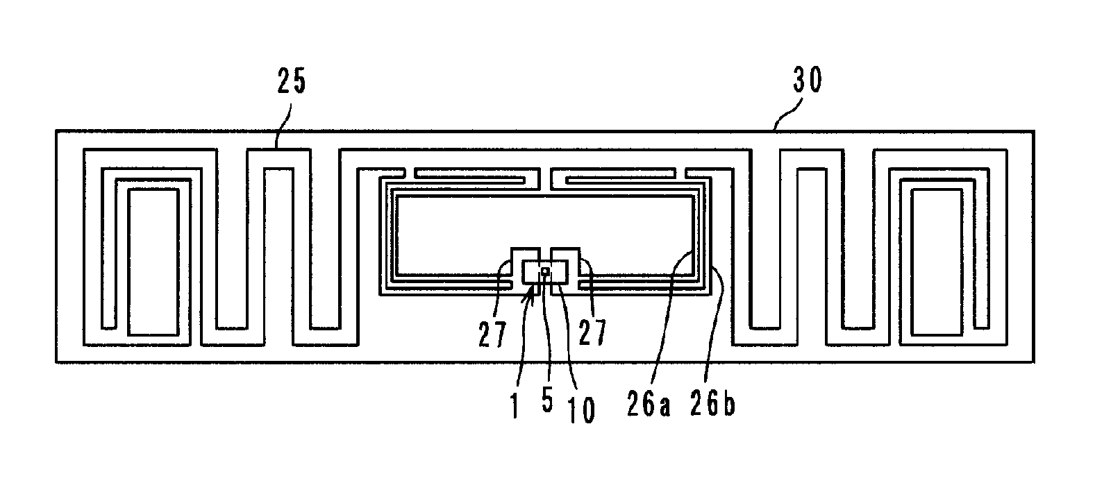
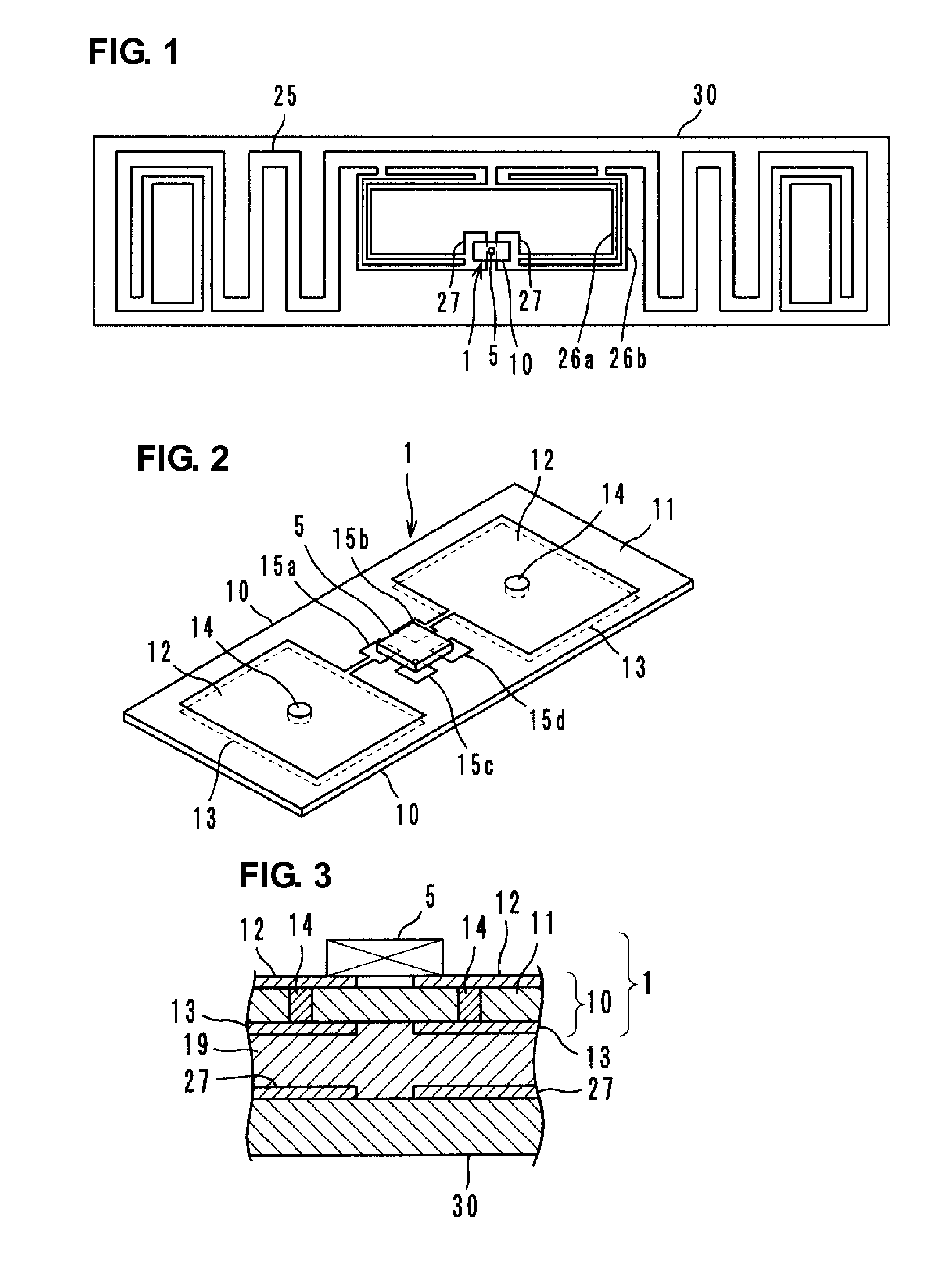
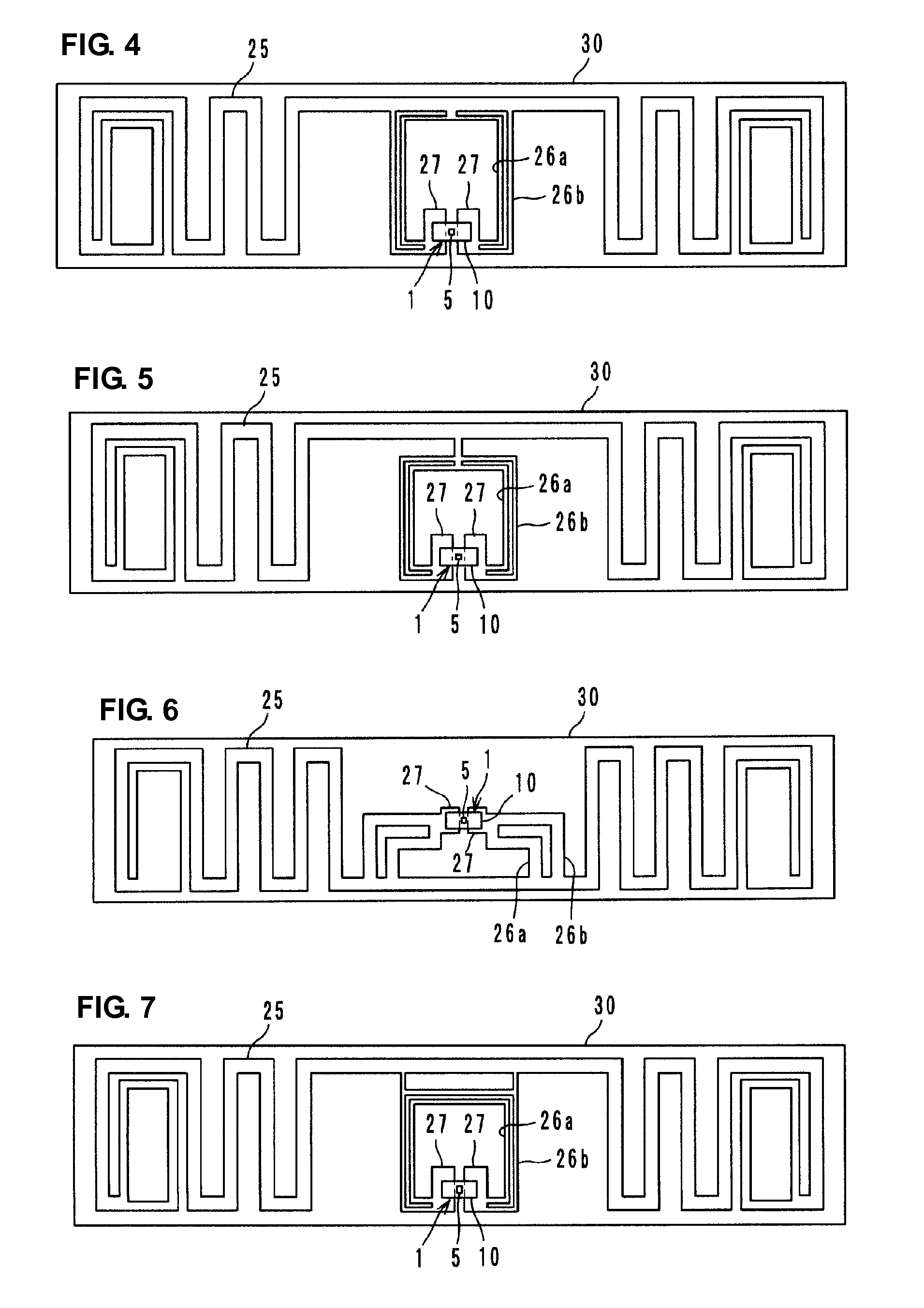
[0035]FIG. 1 to FIG. 3 show a wireless IC device according to a first preferred embodiment of the present invention. This wireless IC device includes an electromagnetic coupling module 1 and a radiation plate 25 disposed on a PET film substrate 30. The electromagnetic coupling module includes a wireless IC chip 5 arranged to process transmission and reception signals of a predetermined frequency and a feeder circuit board 10 having the wireless IC chip 5 mounted thereon.

[0036]In the feeder circuit board 10, a pair of planar electrodes 12 and a pair of planar electrodes 13 are arranged on front and back surfaces of a PET film substrate 11, respectively, so as to face ...


PUM


Abstract

A wireless IC device includes an electromagnetic coupling module, which includes a feeder circuit board having a wireless IC chip arranged to process transmission and reception signals mounted thereon, and a radiation plate. Linear loop electrodes provided in the radiation plate are electromagnetically coupled to planar electrodes located on a surface of the feeder circuit board. A signal received by the radiation plate drives the wireless IC chip. A response signal from the wireless IC chip is transmitted to the outside from the radiation plate. A frequency of the transmission and reception signals is substantially determined by inductance of the loop electrodes, capacitance between the loop electrodes and the planar electrodes, and stray capacitance generated between lines of the loop electrodes.

Description

BACKGROUND OF THE INVENTION[0001]1. Field of the Invention[0002]The present invention relates to wireless IC devices. More particularly, the present invention relates to a wireless-IC-chip containing wireless IC device for use in a radio frequency identification (RFID) system.[0003]2. Description of the Related Art[0004]In recent years, RFID systems have been developed as an article management system in which communication is performed in a contactless manner between a reader / writer that generates an induction field and an IC chip (also referred to as an IC tag and a wireless IC chip) that is affixed to an article or a container and that stores predetermined information, whereby information is exchanged. In the related art, a device disclosed in Japanese Unexamined Patent Application Publication No. 2005-244778 is known as a wireless IC device including an IC chip.[0005]The wireless IC device includes an IC chip, main antenna elements, an auxiliary antenna element, and matching unit...

Claims


Application Information

Patent Timeline
Patent Type & Authority Patents(United States)
IPC IPC(8): G08B13/14
CPCG06K19/07749G06K19/07756G06K19/07786H01Q1/2225H01Q1/38H01Q1/40H01Q9/24H01Q9/26
Inventor KATO, NOBORU
Owner MURATA MFG CO LTD
Why Eureka
Try Eureka