
Group-III nitride semiconductor light emitting device and production method thereof, and lamp

a technology of nitride semiconductor and light emitting device, which is applied in the manufacture of semiconductor/solid-state devices, semiconductor devices, electrical devices, etc., can solve the problems of defective light emitting layer, damage to light emitting layer, and deterioration of semiconductor layer, and achieve excellent crystallinity and high internal quantum efficiency. , the effect of superior electric characteristics

Active Publication Date: 2013-04-16
TOYODA GOSEI CO LTD
View PDF15 Cites 24 Cited by
  • Summary
  • Abstract
  • Description
  • Claims
  • Application Information

AI Technical Summary

Benefits of technology

The present invention relates to a group III nitride semiconductor light emitting device with a flat surface and convex portions. The device is constructed by growing a group III nitride semiconductor layer on the substrate, which includes a principal plane and the convex portions. The base portion width of the convex portions is small, and the surface of the group III nitride semiconductor layer can be planarized rapidly. This results in a high level of crystallinity, reduced dislocations, and excellent light emitting properties without causing leakage current or deteriorations in ESD resistance. The device also exhibits superior electric characteristics and high internal quantum efficiency. The method for producing the device includes a substrate processing step, an epitaxial step, and an LED lamination step. The resulting light emitting device has excellent light confinement and superior light extraction efficiency. The present invention also provides a lamp that uses the light emitting device.

Problems solved by technology

However, in the light emitting device in which an uneven pattern is formed on the light extraction surface by means of mechanical or chemical processing, the processing on the light extraction surface causes overloading on the semiconductor layer, leaving damage in the light emitting layer.
In addition, in the light emitting device in which the semiconductor layer has been grown under such a condition that allows an uneven pattern to be formed on the light extraction surface, the crystallinity of the semiconductor layer is deteriorated, thereby making the light emitting layer defective.
For this reason, when an uneven pattern is formed on the light extraction surface, although the light extraction efficiency improves, the internal quantum efficiency is lowered, causing a problem in that the light emission intensity cannot be increased.

Method used


Image

  • Group-III nitride semiconductor light emitting device and production method thereof, and lamp
  • Group-III nitride semiconductor light emitting device and production method thereof, and lamp
  • Group-III nitride semiconductor light emitting device and production method thereof, and lamp

Examples


examples

[0215]Next, the group III nitride semiconductor light emitting device according to the present invention will be described in more detail below using a series of examples and comparative examples, although the present invention is in no way limited by these examples.

example 7

[0267]By using the group III nitride semiconductor light emitting devices produced in the above Examples 4 to 6, lamps (i.e., packages) each of which installing the aforementioned group III nitride semiconductor light emitting device were prepared in accordance with the method described in Japanese Unexamined Patent Application, First Publication No. 2007-194401. Furthermore, as an example of an electronic device or mechanical device, it was possible to prepare a back light which incorporated the lamp.

experimental example

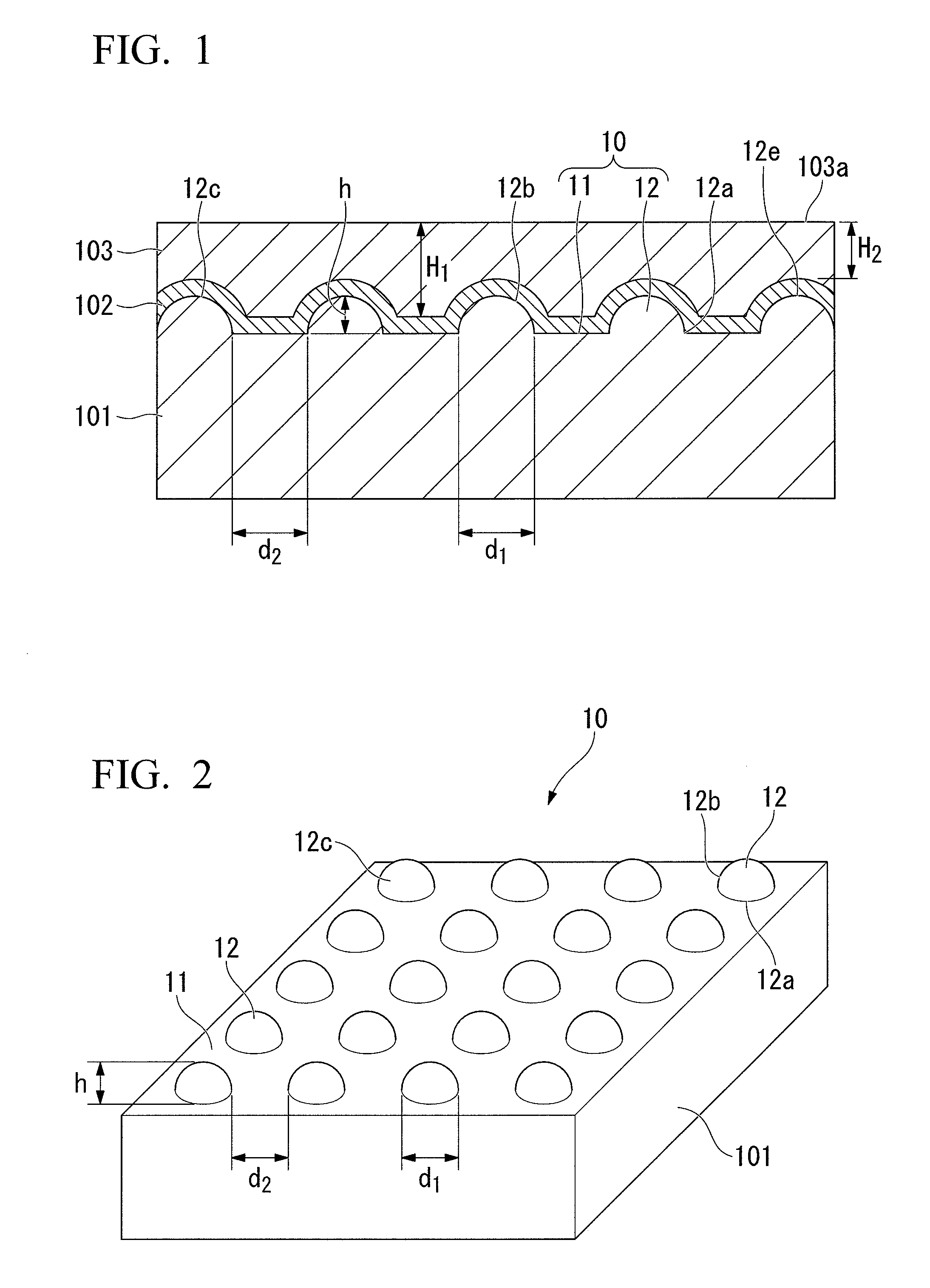
[0268]The square chips of group III nitride semiconductor light emitting devices having a side length of 350 μm were prepared by the same method as that in the above Examples 4 to 6, and the samples of light emitting devices were prepared by mounting the positive electrode bonding pad and the negative electrode bonding pad on a lead frame so that they were facing upwards, and using gold wiring to connect to the lead frame. At this time, the samples having an interval between the convex portions of the substrate in the width direction of 1 μm were assigned to Experimental Example 1, and the samples having an interval between the convex portions of the substrate in the width direction of 2 μm were assigned to Experimental Example 2. Five samples were prepared for each Experimental Example.

[0269]Then, the light emission intensity of each of these samples was measured by moving a detector in the vertical direction with respect to the upper face of the chip, and the measured results are ...


PUM


Abstract

A group III nitride semiconductor light emitting device including an LED structure formed on top of a single crystal, base layer (103) formed on top of a substrate (101) including a principal plane (10) having a flat surface (11) configured from a (0001) C plane, and a plurality of convex portions (12) including a surface (12c) non-parallel to the C plane having a width (d1) of 0.05 to 1.5 μm and height (H) of 0.05 to 1 μm, the base layer is formed by causing a group III nitride semiconductor to grow epitaxially so as to cover the flat surface and convex portions, and the width (d1) of the convex portions and top portion thickness (H2) of the base layer at the positions of the top portions (12e) of the convex portions satisfy: H2=kd1 (wherein 0.5<k<5, and H2=0.5 μm or more).

Description

TECHNICAL FIELD[0001]The present invention relates to a group III nitride semiconductor light emitting device that has a light emitting diode (LED) structure and a production method thereof, and also relates to a lamp.[0002]Priority is claimed on Japanese Patent Application No. 2008-162485, filed Jun. 20, 2008, the content of which is incorporated herein by reference.BACKGROUND ART[0003]In recent years, a group III nitride semiconductor light emitting device has been attracting attention as a semiconductor material for light emitting devices which emit light of short wavelength. A group III nitride semiconductor is represented by the general formula AlxGayInzN (0≦x≦1, 0≦y≦1, 0≦z≦1 and x+y+z=1), and is formed on top of a substrate made of a sapphire single crystal, various kinds of oxides, or a group III-V compound, through a metal organic chemical vapor deposition method (MOCVD method), a molecular beam epitaxy method (MBE method), or the like.[0004]In a typical light emitting devic...

Claims


Application Information

Patent Timeline
Patent Type & Authority Patents(United States)
IPC IPC(8): H01L33/20H01L33/32H01L33/00H01L33/12H01L33/22
CPCH01L33/16H01L33/007H01L33/12H01L21/0237H01L21/0243H01L21/02433H01L21/02458H01L21/0254
Inventor SHINOHARA, HIRONAOSAKAI, HIROMITSU
Owner TOYODA GOSEI CO LTD
Learn More