In chamber sodium doping process and system for large scale cigs based thin film photovoltaic materials

a photovoltaic material and sodium doping technology, applied in the direction of vacuum evaporation coating, semiconductor devices, coatings, etc., can solve the problems of petrochemical fuel supply limitation, rapid becoming a scarce resource, and depletion

Inactive Publication Date: 2013-04-23
CM MFG
View PDF287 Cites 61 Cited by
  • Summary
  • Abstract
  • Description
  • Claims
  • Application Information

AI Technical Summary

Benefits of technology

[0011]In another specific embodiment, the present invention provides a method of processing a photovoltaic materials using a sputtering process. The method includes providing at least one transparent substrate having an overlying first electrode layer. The method includes forming an overlying copper and gallium layer from a first target including a copper species and a gallium species using a first sputtering process within a first chamber. Additionally, the method includes forming an indium layer overlying the copper and the gallium layer from a second target including an indium species using a second sputtering process within the first chamber. The method further includes transferring the transparent substrate including the indium layer overlying the copper la...

Problems solved by technology

Unfortunately, the supply of petrochemical fuel is limited and essentially fixed based upon the amount available on the planet Earth.
Additionally, as more people use petroleum products in growing amounts, it is rapidly becoming a scarce resource, which will eventually become depleted over time.
Although solar energy is environmentally clean and has been successful to a point, many limitations remain to be resolved before it becomes widely used throughout the world.
However, crystalline materials are often costly and difficult to make on a large scale.
Additionally, devices mad...

Method used


Image

  • In chamber sodium doping process and system for large scale cigs based thin film photovoltaic materials
  • In chamber sodium doping process and system for large scale cigs based thin film photovoltaic materials
  • In chamber sodium doping process and system for large scale cigs based thin film photovoltaic materials

Examples


Embodiment Construction

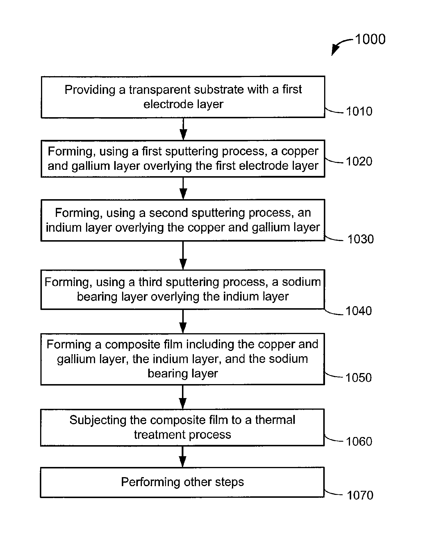
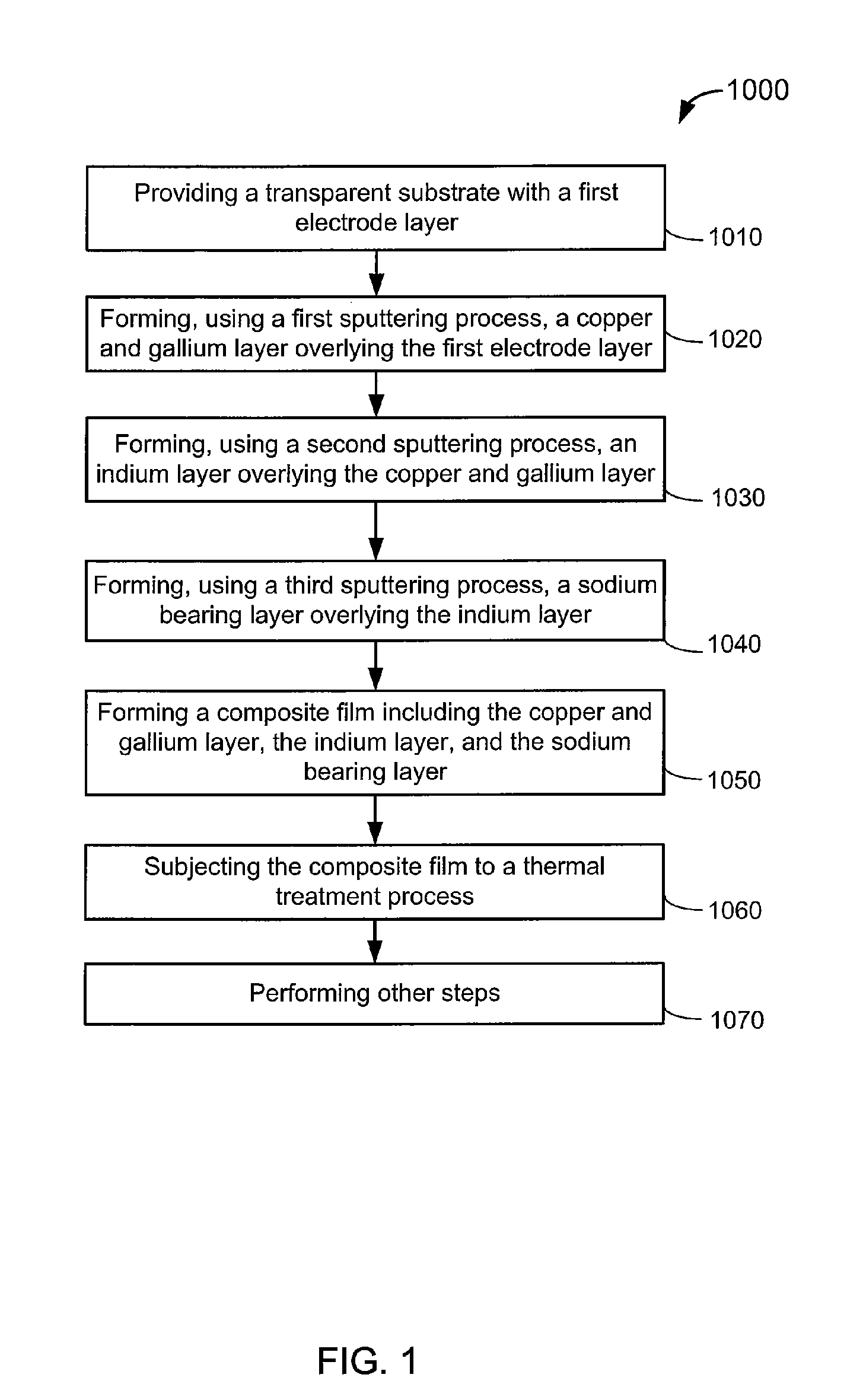
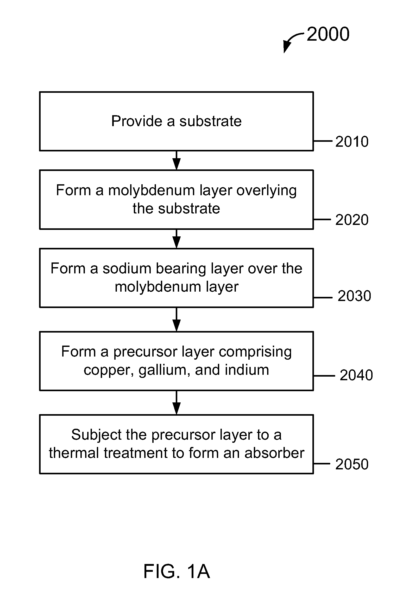
[0017]The present invention relates generally to photovoltaic materials and manufacturing method. More particularly, the present invention provides a method and structure for fabricating a thin film solar cells. Merely by way of example, the present method includes in-chamber sodium doping for manufacture of chalcopyrite structured thin film photovoltaic cells base on a large scale batch system, but it would be recognized that the invention may have other configurations.

[0018]FIG. 1 is a simplified flowchart illustrating a method of fabricating a thin film photovoltaic cell according to an embodiment of the present invention. This diagram is merely an example, which should not unduly limit the scope of the claims herein. The method 1000 includes the following processes:

[0019]1. Process 1010 for providing a transparent substrate overlaid with a first electrode layer;

[0020]2. Process 1020 for forming, using a first sputtering process within a first chamber, a copper and gallium layer ...


PUM

PropertyMeasurementUnit
Temperatureaaaaaaaaaa
Compositionaaaaaaaaaa
Concentrationaaaaaaaaaa

Abstract

A method of processing a photovoltaic materials using a sputtering process including providing at least one transparent substrate having an overlying first electrode layer. The method further including forming an overlying copper and gallium layer using a first sputtering process within a first chamber from a first target including a copper species and a gallium species. Additionally, the method includes forming an indium layer overlying the copper and the gallium layer using a second sputtering process within the first chamber from a second target including an indium species. The method further includes forming a sodium bearing layer overlying the indium layer using a third sputtering process within the first chamber, thereby forming a composite film including the copper and gallium layer, the indium layer, and the sodium bearing layer. Furthermore, the method includes subjecting the composite film to at least a thermal treatment process to form a chalcopyrite absorber layer comprising copper, indium, gallium, and sodium therein.

Description

CROSS-REFERENCES TO RELATED APPLICATIONS[0001]This application claims priority to U.S. Provisional Patent Application No. 61 / 101,638, filed Sep. 30, 2008, entitled “IN CHAMBER SODIUM DOPING PROCESS AND SYSTEM FOR LARGE SCALE CIGS BASED THIN FILM PHOTOVOLTAIC MATERIALS” by inventor Robert D. Wieting, commonly assigned and incorporated by reference herein for all purposes.STATEMENT AS TO RIGHTS TO INVENTIONS MADE UNDER FEDERALLY SPONSORED RESEARCH AND DEVELOPMENT[0002]Not ApplicableREFERENCE TO A “SEQUENCE LISTING,” A TABLE, OR A COMPUTER PROGRAM LISTING APPENDIX SUBMITTED ON A COMPACT DISK[0003]Not ApplicableBACKGROUND OF THE INVENTION[0004]The present invention relates generally to photovoltaic materials and manufacturing method. More particularly, the present invention provides a method and structure for fabricating a thin film solar cells. Merely by way of example, the present method includes in-chamber sodium doping for manufacture of chalcopyrite structured thin film photovoltai...

Claims


Application Information

Patent Timeline
IPC IPC(8): C23C14/32C23C14/00
CPCH01L31/022425H01L31/0322H01L31/03923H01L21/02491H01L21/02579H01L21/02614H01L21/02631H01L21/02568Y02E10/541
Inventor WIETING, ROBERT D.
Owner CM MFG
Why Eureka
Try Eureka