Semiconductor device and production method thereof

a technology of semiconductors and production methods, applied in the direction of semiconductor devices, electrical devices, transistors, etc., can solve the problems of prolonged development period and undesired production cost increase, and achieve high operation speed, high rewrite cycle, and high reliability

Inactive Publication Date: 2013-05-28
RENESAS ELECTRONICS CORP
View PDF9 Cites 10 Cited by
  • Summary
  • Abstract
  • Description
  • Claims
  • Application Information

AI Technical Summary

Benefits of technology

[0011]In the case of a split gate type memory in which a memory gate electrode is formed in the shape of a sidewall over a sidewall on one side of a control gate electrode, the length of the memory gate electrode is decided in accordance with the thickness of a gate polysilicon film in a self-aligning manner. That is, since the length of the memory gate electrode is decided in accordance with the thickness of a polysilicon film, it is desired to improve a technology of forming different memory gate lengths in an identical chip with a high degree of accuracy.
[0012]In view of the above situation, the present inventors have studied a method for selectively forming memory gate lengths in an identical chip accurately and easily and jointly loading memory cells having plural kinds of performance over the identical chip.
[0013]An object of the present invention is to provide a semiconductor device having a nonvolatile memory cell of a high operation speed and a high rewrite cycle and a nonvolatile memory cell of high reliability by jointly loading memory cells having different memory gate lengths in an identical chip.
[0014]Another object of the present invention is to provide a technology that can: shorten the development period of a semiconductor device having nonvolatile memory cells; and reduce the chip area at a low cost.
[0019]By jointly loading memory cells having different memory gate lengths in an identical chip, it is possible to provide a semiconductor device having a nonvolatile memory cell of a high operation speed and a high rewrite cycle and a nonvolatile memory cell of high reliability.
[0020]Further, it is possible to shorten the development period of a semiconductor device having nonvolatile memory cells and reduce the chip area at a low cost.

Problems solved by technology

In order to meet all the requests with a single kind of a memory cell however, it is necessary for example to develop a memory having a high operation speed, a high rewrite cycle, high reliability, and very high performance, but on this occasion the development period prolongs and the production cost increases undesirably.

Method used


Image

  • Semiconductor device and production method thereof
  • Semiconductor device and production method thereof
  • Semiconductor device and production method thereof

Examples


embodiment 1

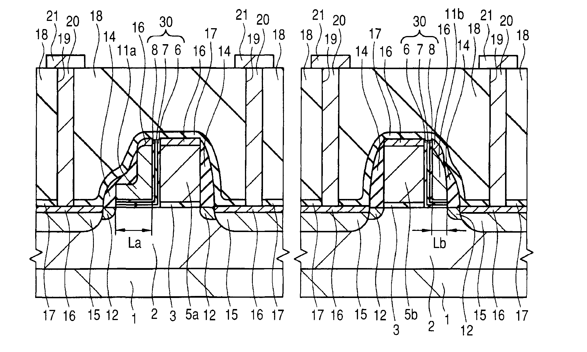
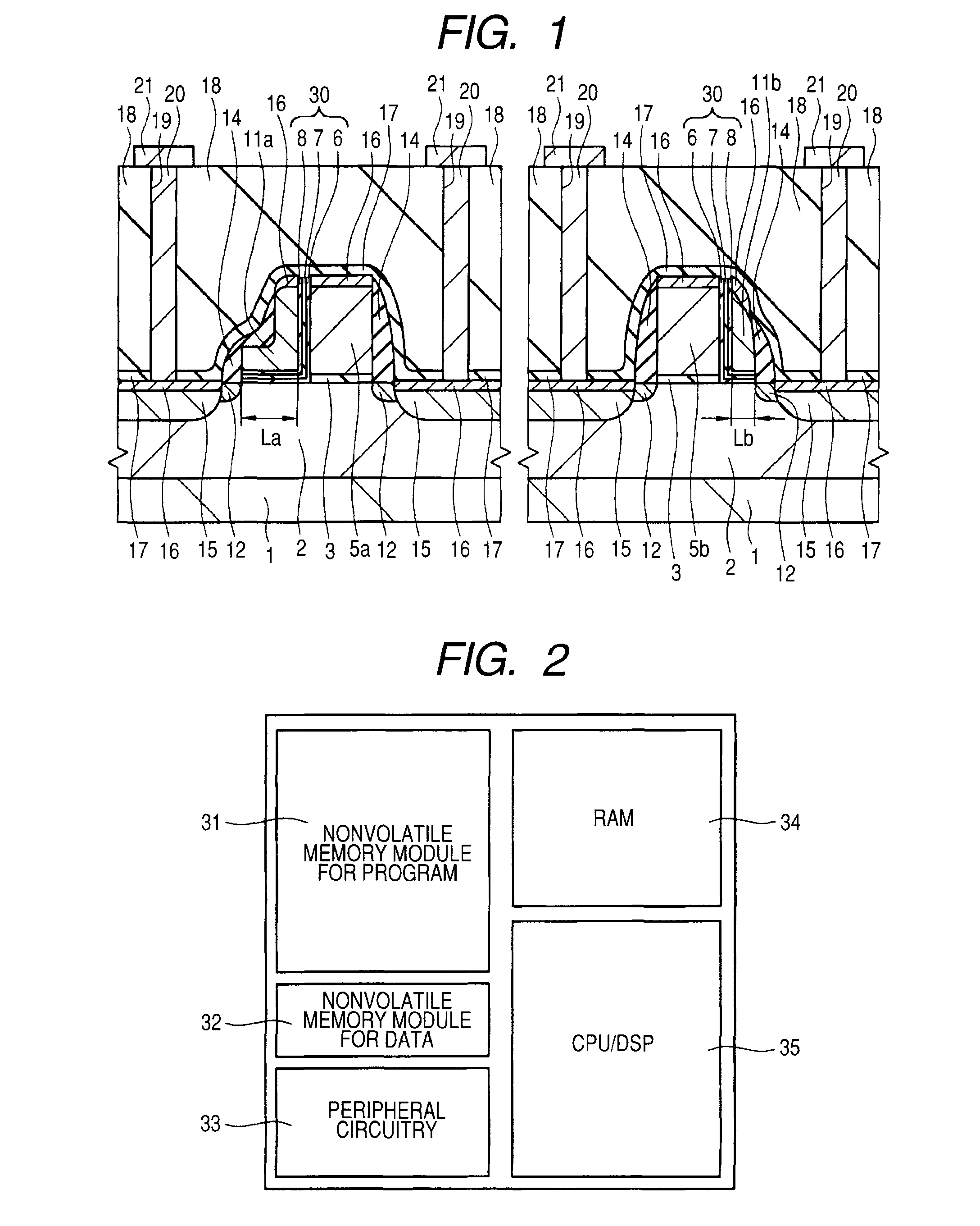
[0056]FIG. 1 is a sectional view showing a substantial part in a memory alley region of a semiconductor device according to Embodiment 1 of the present invention. FIG. 2 is a plan view showing the layout of the semiconductor device according to Embodiment 1 of the present invention and the microcomputer is equipped with a nonvolatile memory module 31 for programs, a nonvolatile memory module 32 for data, a peripheral circuit 33, a RAM (Random Access Memory) 34, and a CPU (Central Processing Unit) / DSP (Digital Signal Processor) 35.

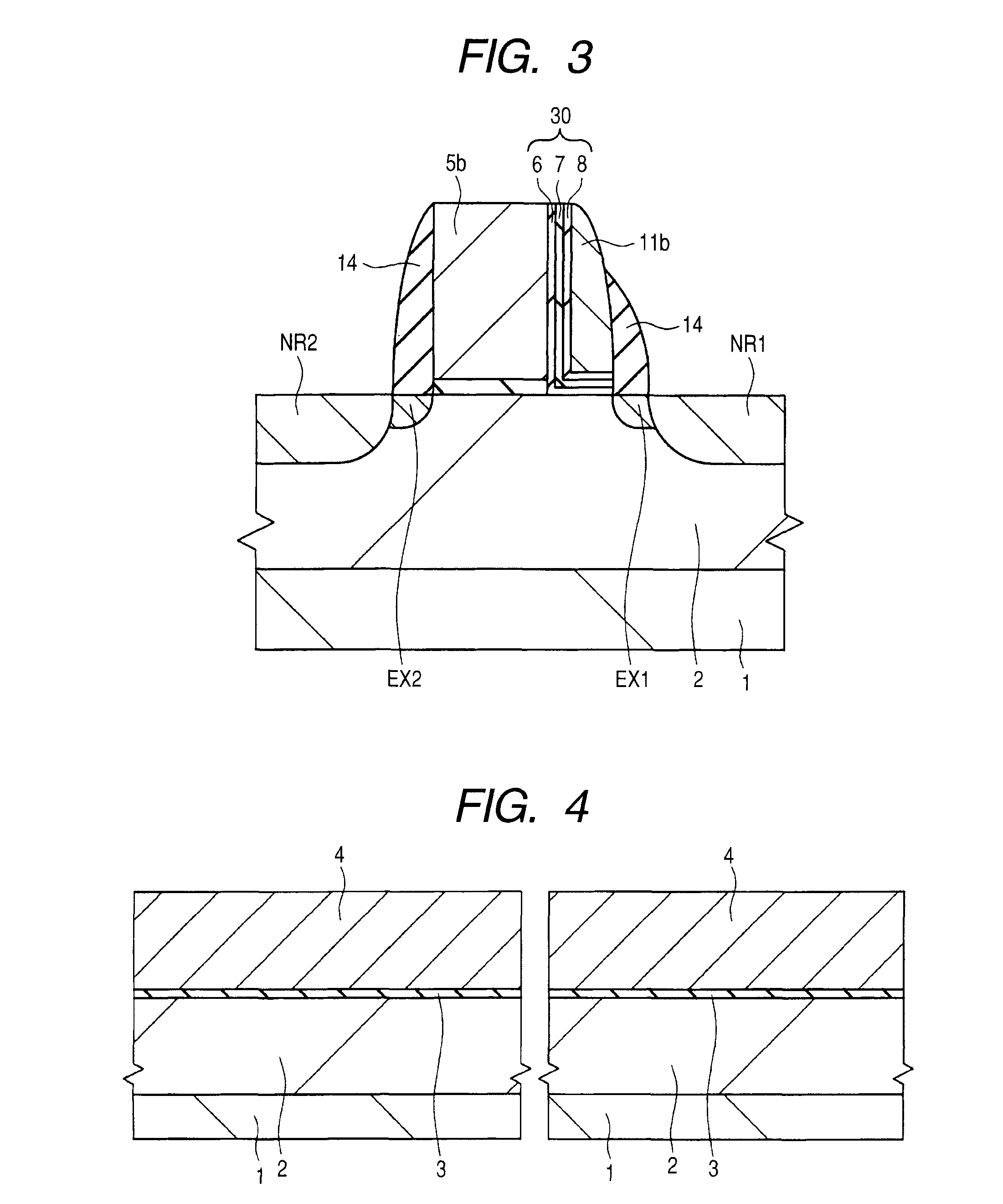
[0057]The semiconductor device according to the present embodiment includes a nonvolatile semiconductor memory device having split gate type memory cells of a MONOS type. The split gate type memory cells of the present embodiment comprise control MIS transistors and memory MIS transistors which are formed over a p-type well 2 in a p-type silicon substrate 1, as shown in FIG. 1. Gate electrodes of the control MIS transistors (control gate electrodes 5a and 5...

embodiment 2

[0086]A method for producing nonvolatile memories according to the present embodiment is hereunder explained in the order of the process steps in reference to FIGS. 15 to 21.

[0087]Firstly, as shown in FIG. 15, in the same way as Embodiment 1, a gate insulation film 3 and control gate electrodes 5a and 5b are formed respectively over the main face of a silicon substrate 1 having a p-type well 2. Thereafter an ONO film 30, a polycrystalline silicon film 9, and a silicon oxide film 10 are deposited sequentially over the main face of the silicon substrate 1 and parts of the silicon oxide film 10 are removed by dry etching in which a photolithography technology is used so that the silicon oxide film 10 may remain over the polycrystalline silicon film 9 formed over the sidewalls of the control gate electrode 5a. That is, the silicon oxide film 10 over the polycrystalline silicon film 9 formed over the sidewalls of the control gate electrode 5b is removed. Thereafter, the remaining silicon...

embodiment 3

[0100]A method for producing nonvolatile memories according to the present embodiment is hereunder explained in the order of the process steps in reference to FIGS. 22 to 26.

[0101]Firstly, as shown in FIG. 22, in the same way as Embodiment 1, a gate insulation film 3 and control gate electrodes 5a and 5b are formed respectively over the main face of a silicon substrate 1 having a p-type well 2. Thereafter an ONO film 30 and a polycrystalline silicon film 9 are deposited sequentially over the main face of the silicon substrate 1.

[0102]Successively, as shown in FIG. 23, a photoresist film 22 is formed over the main face of the silicon substrate 1 and, on this occasion, the photoresist film 22 is formed so that only the vicinity of the sidewall on one side of the control gate electrode 5a may be covered with the photoresist film 22.

[0103]Successively, as shown in FIG. 24, parts of the polycrystalline silicon film 9 are removed by dry etching. On this occasion, over the sidewall of the ...


PUM


Abstract

An object of the present invention is to provide a semiconductor device having a nonvolatile memory cell of a high operation speed and a high rewrite cycle and a nonvolatile memory cell of high reliability. In a split gate type nonvolatile memory in which memory gate electrodes are formed in the shape of sidewalls of control gate electrodes, it is possible to produce a memory chip having a memory of a high operation speed and a high rewrite cycle and a memory of high reliability at a low cost by jointly loading memory cells having different memory gate lengths in an identical chip.

Description

CROSS-REFERENCE TO RELATED APPLICATIONS[0001]The disclosure of Japanese Patent Application No. 2009-132668 filed on Jun. 2, 2009 including the specification drawings and abstract is incorporated herein by reference in its entirety.BACKGROUND OF THE INVENTION[0002]The present invention relates: to a semiconductor device and a production method thereof; and in particular to a technology effectively applied to a semiconductor device having a nonvolatile memory cell a memory gate electrode of which is formed over the sidewall of a control gate electrode and a production method thereof.[0003]A semiconductor device formed by jointly loading an electrically rewritable nonvolatile memory and a microcomputer over a single silicon substrate is widely used as an embedded microcomputer for an industrial machine, a household appliance, an in-vehicle device, or the like.[0004]A nonvolatile memory in such a semiconductor device is used by storing and occasionally retrieving a program required by a...

Claims


Application Information

Patent Timeline
Patent Type & Authority Patents(United States)
IPC IPC(8): H01L29/788
CPCH01L21/28273H01L27/11521H01L29/42324H01L29/7887H01L29/66833H01L29/42344H01L29/792H01L29/40117H10B43/30
Inventor KAWASHIMA, YOSHIYUKI
Owner RENESAS ELECTRONICS CORP
Why Eureka
Try Eureka