Hetero resistive switching material layer in RRAM device and method

a resistive switching and material layer technology, applied in semiconductor devices, digital storage, instruments, etc., can solve the problems of increasing power dissipation, non-scaling of sub-threshold slopes, and reducing device performance, so as to improve the performance of resistive switching devices and widen the range of applicability

Active Publication Date: 2013-06-18
CROSSBAR INC
View PDF164 Cites 72 Cited by
  • Summary
  • Abstract
  • Description
  • Claims
  • Application Information

AI Technical Summary

Benefits of technology

[0007]The present invention is directed to switching device. More particularly, the present invention is directed to a resistive switching device having more than one switching material to enhance performance of the resistive switching device. For example, the resistive switching device can include a first switching material for switching and a second material for suppressing leakage current when an operating voltage is applied. Embodiments according to the present invention can be particularly useful for a non-volatile memory device in an interconnected device array. It should be recognized, however, that embodiments according to the present invention can have a much broader range of applicability.

Problems solved by technology

However, as field effect transistors (FET) approach sizes less than 100 nm, problems such as short channel effect can degrade device performance.
Moreover, such sub 100 nm device size can lead to sub-threshold slope non-scaling and also increases power dissipation.
These devices often require new materials and device structures to couple with silicon-based devices to form a memory cell, which lack one or more key attributes.
For example, FeRAM and MRAM devices have fast switching characteristics and good programming endurance, but their fabrication is not CMOS compatible and size is usually large.
Organic RAM is incompatible with large volume silicon-based fabrication and device reliability is usually poor.

Method used


Image

  • Hetero resistive switching material layer in RRAM device and method
  • Hetero resistive switching material layer in RRAM device and method
  • Hetero resistive switching material layer in RRAM device and method

Examples


Embodiment Construction

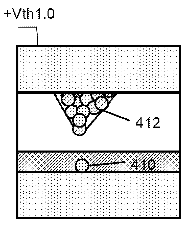
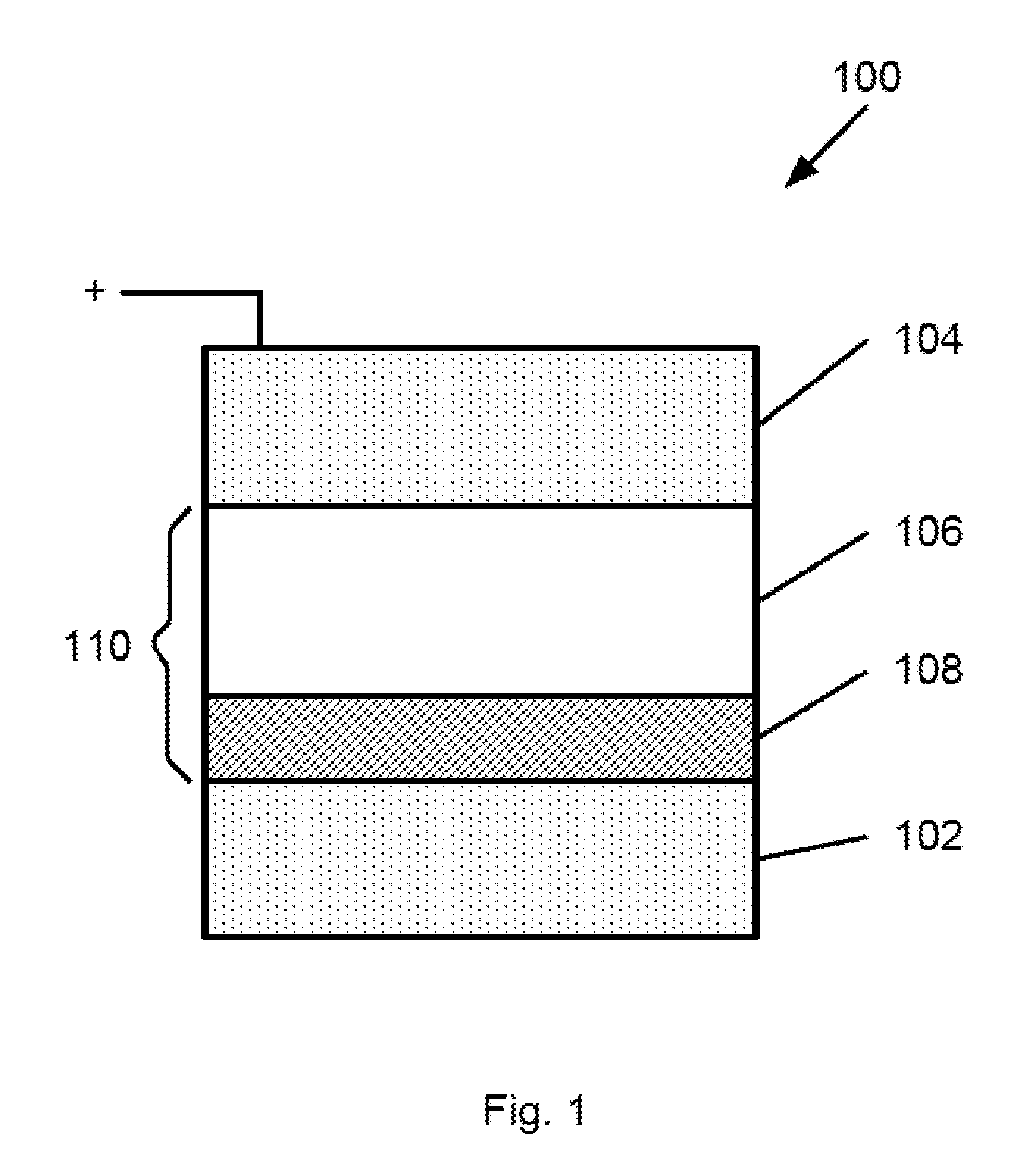
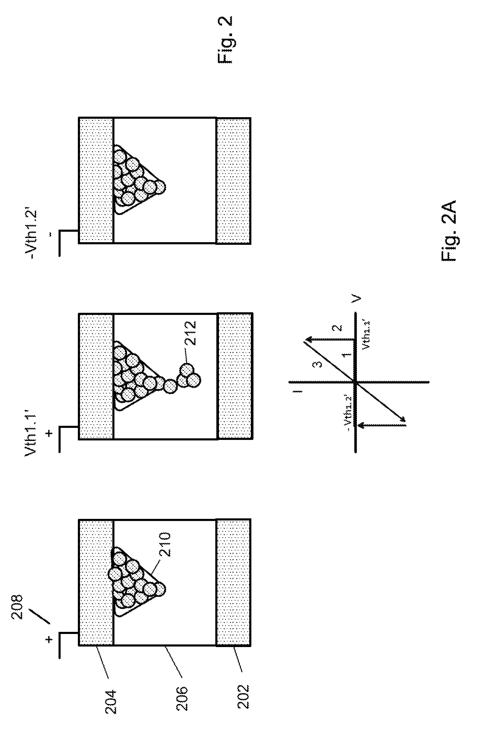
[0038]The present invention is directed to switching device. More particularly, the present invention is directed to a resistive switching device having more than one switching material to enhance performance of the resistive switching device. For example, the resistive switching device can include a first switching material for switching and a second material for suppressing leakage current when an operating voltage is applied. Embodiments according to the present invention can be particularly useful for a non-volatile memory device in an interconnected device array. It should be recognized that embodiments according to the present invention can have a much broader range of applicability.

[0039]High density and low cost storage devices are in ever increasing demand due to the growth in consumer devices common in the market place. Current non-volatile memory devices including Flash are probably at an end to further scaling due to fundamental limitations in the devices. It is predicte...


PUM


Abstract

A non-volatile memory device includes a first electrode, a resistive switching material stack overlying the first electrode. The resistive switching material stack comprising a first resistive switching material and a second resistive switching material. The second resistive switching material overlies the first electrode and the first resistive switching material overlying the second resistive switching material. The first resistive switching material is characterized by a first switching voltage having a first amplitude. The second resistive switching material is characterized by a second switching voltage having a second amplitude no greater than the first switching voltage. A second electrode comprising at least a metal material physically and electrically in contact with the first resistive switching material overlies the first resistive switching material.

Description

CROSS REFERENCE TO RELATED APPLICATIONS[0001]Not ApplicableSTATEMENTS RELATED TO FEDERAL OR GOVERNMENT SPONSORED RESEARCH[0002]Not ApplicableBACKGROUND[0003]The present invention is related to switching devices. More particularly, the present invention provides a resistive switching device characterized by a controllable programming current with faster operation speed. Embodiments of the present invention have been applied to fabrication and operation of a resistive random access memory device. But it should be recognized that the present invention can have a much broader range of applicability.[0004]The success of semiconductor devices has been mainly driven by an intensive transistor down-scaling process. However, as field effect transistors (FET) approach sizes less than 100 nm, problems such as short channel effect can degrade device performance. Moreover, such sub 100 nm device size can lead to sub-threshold slope non-scaling and also increases power dissipation. It is generall...

Claims


Application Information

Patent Timeline
Patent Type & Authority Patents(United States)
IPC IPC(8): G11C11/00
CPCG11C13/0007G11C13/004G11C13/0069G11C13/0097G11C13/0002H01L45/12H01L45/085H01L45/1266H01L45/14H01L27/2463G11C2013/0073G11C2213/15G11C2213/33G11C2013/0092H10B63/80H10N70/245H10N70/8416H10N70/881H10N70/801
Inventor JO, SUNG HYUN
Owner CROSSBAR INC
Why Eureka
Try Eureka