

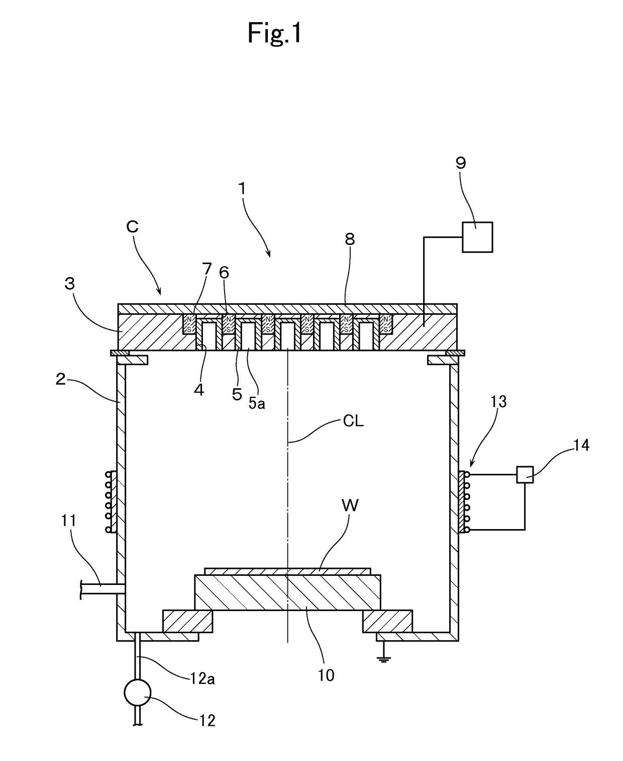
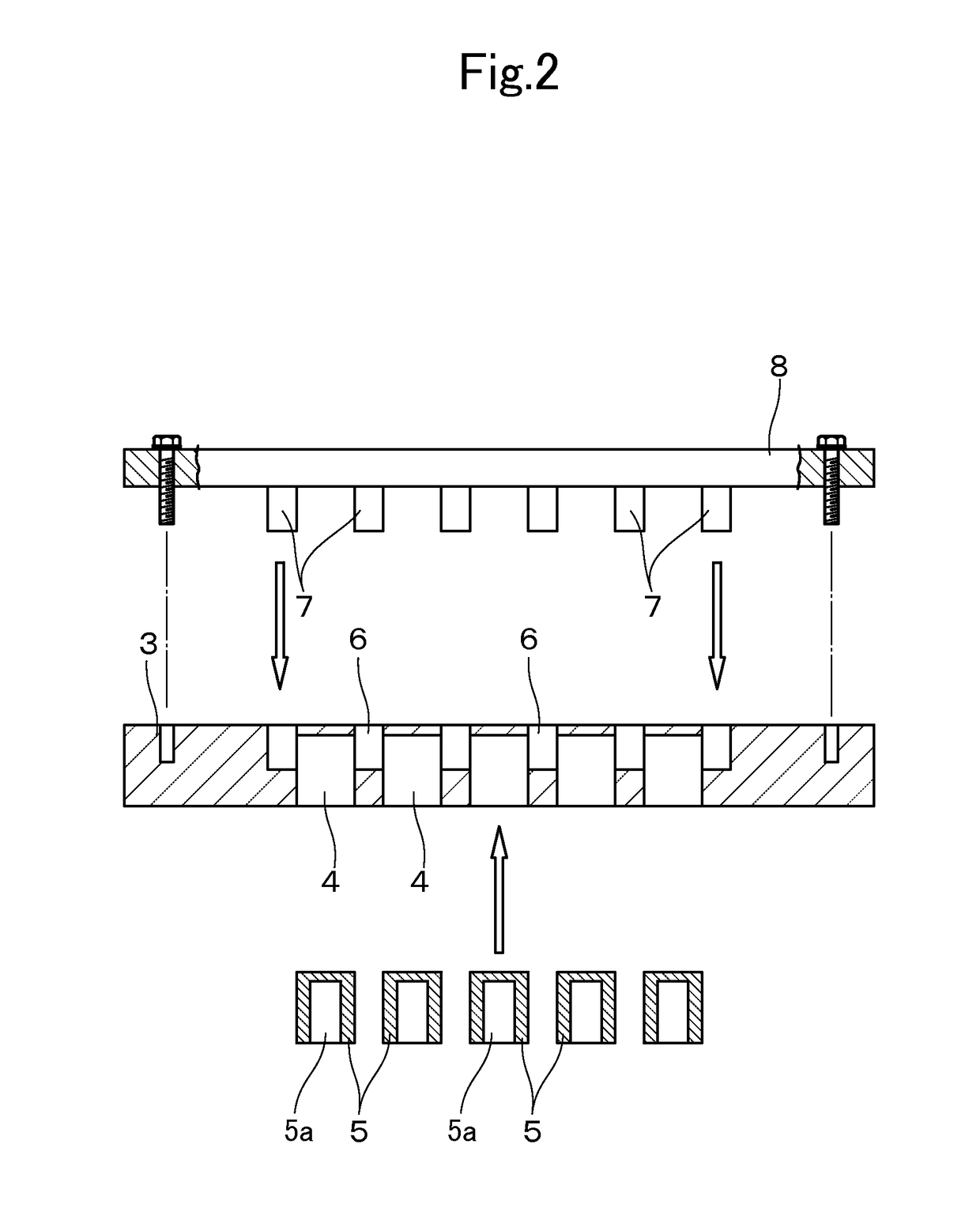
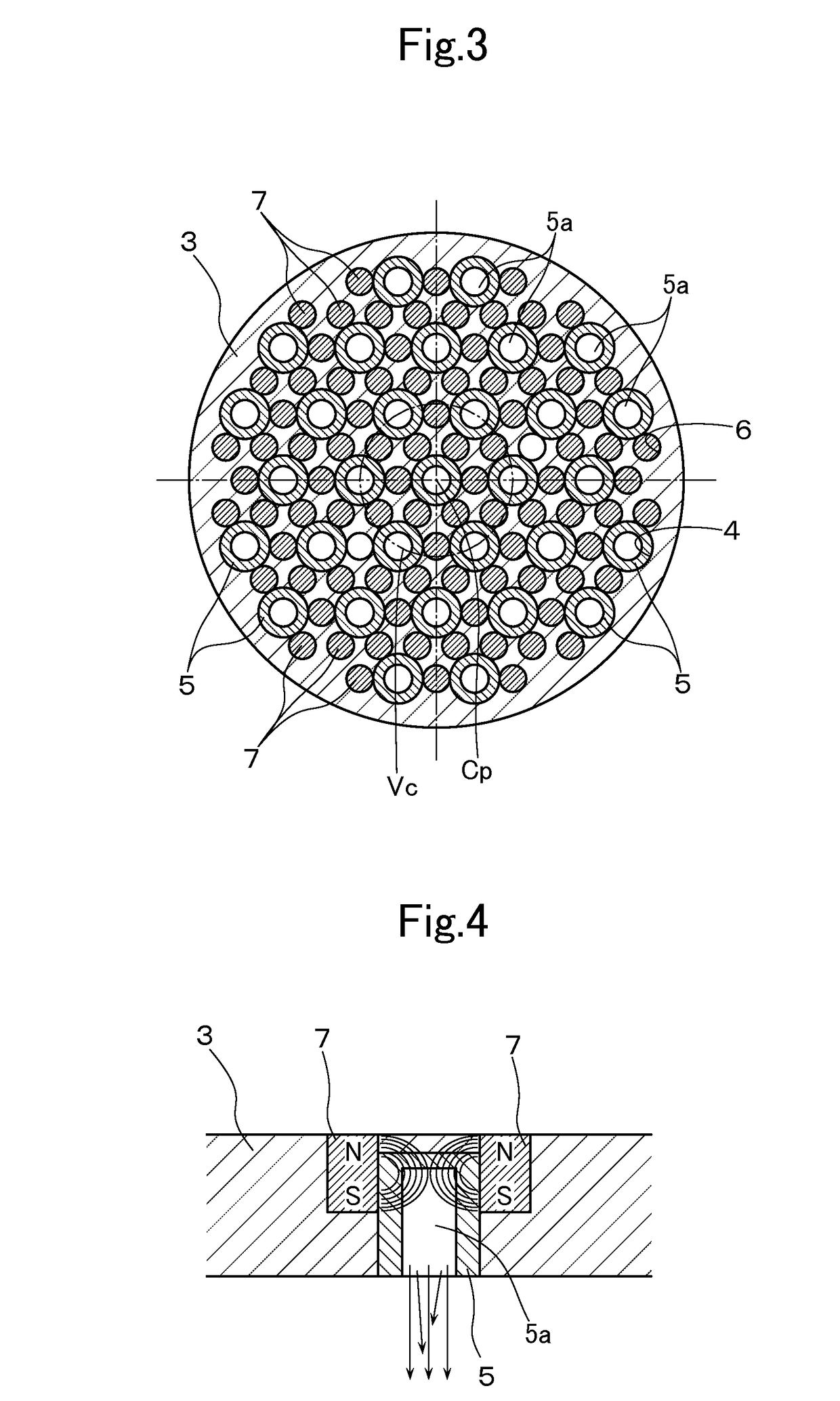
Cathode unit and sputtering apparatus provided with the same
a technology of cathode unit and sputtering apparatus, which is applied in the direction of vacuum evaporation coating, electrolysis components, coatings, etc., can solve the problems of increasing the number of parts, complicated arrangement of the apparatus, and asymmetry in coverage especially in the peripheral portion of the substrate, so as to improve the coating characteristics, reduce the cost of manufacturing the apparatus, and high film thickness
- Summary
- Abstract
- Description
- Claims
- Application Information
AI Technical Summary
Benefits of technology
Problems solved by technology
Method used
Image

Examples
example 1
[0037]In Example 1, a Cu film was formed by using the sputtering apparatus shown in FIG. 1. As the substrate W, there was used one in which, after having formed a silicon oxide film throughout the entire surface of the Si wafer of 300 mm in diameter, the silicon oxide film was subjected to patterning to thereby form micropores (40 nm in width, 140 nm in depth) in the silicon oxide film in a known method.
[0038]As the cathode unit, as shown in FIG. 6, there was used a holder made of copper in a composition ratio of 99% and 200 mm in diameter. In the bottom central portion of the cathode unit, a recessed portion was formed into an opening of 40 mm in diameter and a depth of 50 mm, so as to perform a dual function also of the target member. On the periphery of the recessed portion, six magnet units were built in circumferentially at an equal distance to one another, thus making the cathode unit C1 of Example 1. In this case, the magnet units were arranged such that two magnets were disp...
PUM
| Property | Measurement | Unit |
|---|---|---|
| diameter | aaaaa | aaaaa |
| diameter | aaaaa | aaaaa |
| diameter | aaaaa | aaaaa |
Abstract
Description
Claims
Application Information