Carbon field effect transistors having charged monolayers to reduce parasitic resistance

a field effect transistor and charged monolayer technology, applied in thermoelectric devices, solid-state devices, nanoinformatics, etc., can solve the problems of channel not being doped by conventional methods, performance bottlenecks, and circuit performance degradation, so as to reduce parasitic resistance and reduce parasitic resistance

Active Publication Date: 2013-06-25
GLOBALFOUNDRIES US INC
View PDF61 Cites 22 Cited by
  • Summary
  • Abstract
  • Description
  • Claims
  • Application Information

AI Technical Summary

Benefits of technology

[0005]Aspects of the invention include carbon transistor devices having channels formed from carbon nanostructures, such as carbon nanotubes or graphene, and charged monolayers to reduce parasitic resistance in un-gated regions of the channels, and methods for fabricating carbon transistor devices having charged monolayers to reduce parasitic resistance.

Problems solved by technology

However, the overlap between the source / drain electrodes and the gate electrode results in parasitic capacitance, which degrades the circuit performance.
To reduce this parasitic capacitance, some conventional FET structures having carbon nanotube or graphene channels are formed having non-overlapping source / drain and gate electrodes With these structures, a performance bottleneck arises due to a high parasitic resistance in the un-gated portion of the channel that results from the underlap between the source / drain electrodes and the gate.
However, with graphene and carbon nanotube FET devices, the channel cannot be doped by conventional methods.

Method used


Image

  • Carbon field effect transistors having charged monolayers to reduce parasitic resistance
  • Carbon field effect transistors having charged monolayers to reduce parasitic resistance
  • Carbon field effect transistors having charged monolayers to reduce parasitic resistance

Examples


Embodiment Construction

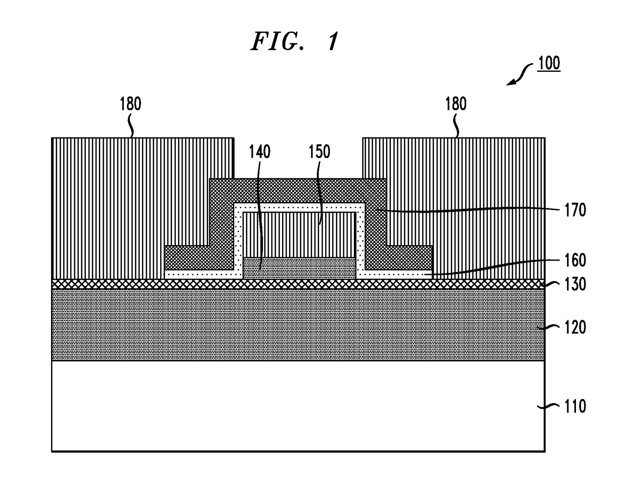
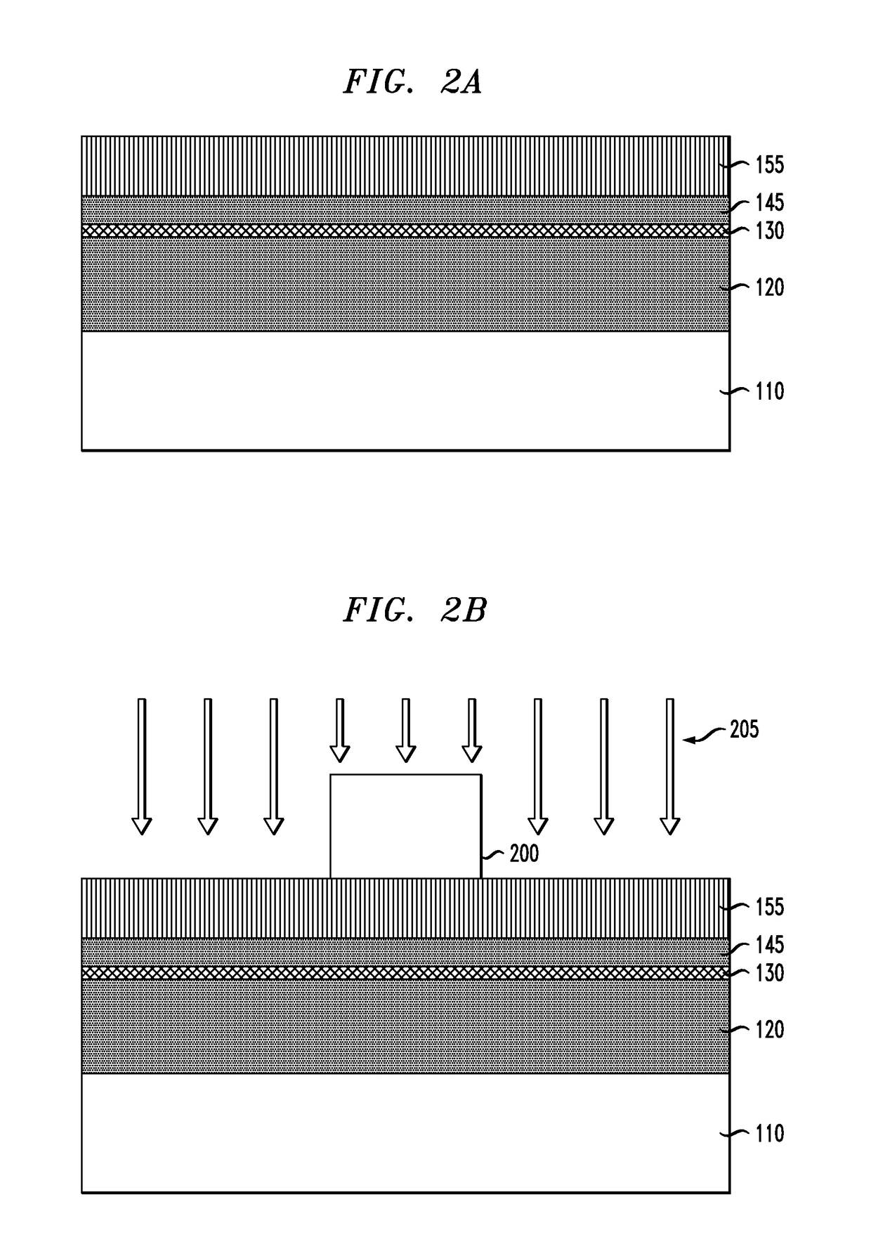
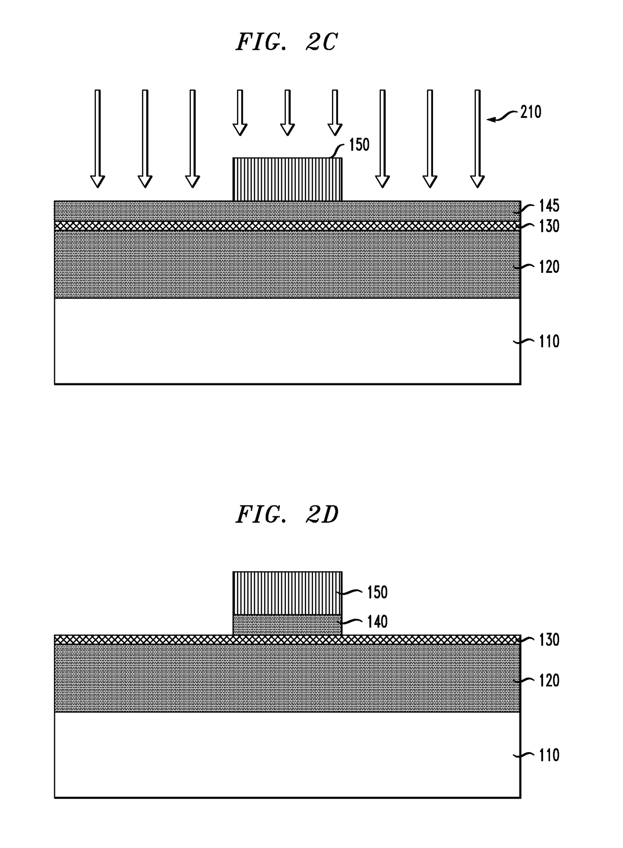
[0023]Preferred embodiments of the invention will now be described in further detail with reference to transistor devices having channels formed from carbon nanostructures, such as carbon nanotubes or graphene, and charged monolayers to reduce parasitic resistance of the channels, and methods for fabricating the transistor devices. It is to be understood that the invention is not limited to the particular materials, features, and processing steps shown and described herein. Modifications to the illustrative embodiments will become apparent to those of ordinary skill in the art. It should also be understood that the various layers and / or regions shown in the accompanying figures are not drawn to scale, and that one or more semiconductor layers and / or regions of a type commonly used in such integrated circuits may not be explicitly shown in a given figure for ease of explanation. Particularly with respect to processing steps, it is to be emphasized that the descriptions provided herei...


PUM

PropertyMeasurementUnit
thicknessaaaaaaaaaa
thicknessaaaaaaaaaa
thicknessaaaaaaaaaa

Abstract

Carbon transistor devices having channels formed from carbon nanostructures, such as carbon nanotubes or graphene, and having charged monolayers to reduce parasitic resistance in un-gated regions of the channels, and methods for fabricating carbon transistor devices having charged monolayers to reduce parasitic resistance. For example, a carbon field effect transistor includes a channel comprising a carbon nanostructure formed on an insulating layer, a gate structure formed on the channel, a monolayer of DNA conformally covering the gate structure and a portion of the channel adjacent the gate structure, an insulating spacer conformally formed on the monolayer of DNA, and source and drain contacts connected by the channel.

Description

TECHNICAL FIELD[0001]This invention relates generally to carbon field effect transistors having charged monolayers to reduce parasitic resistance, and methods for constructing carbon field effect transistors having charged monolayers to reduced parasitic resistance.BACKGROUND[0002]The integration of carbon nanostructures as channel materials in the next generation of electronic devices offers many advantages over the continued scaling of silicon (Si). Carbon nanostructures such as carbon nanotubes and graphene are two nanoscale forms of carbon that exhibit extremely high current carrying capacity and mobilities, which are several orders of magnitude beyond the theoretical limit for Si. Furthermore, carbon nanotubes (one-dimensional) and graphene (two-dimensional) are low-dimensional (ultra-thin-body) materials, which allows them to be aggressively scaled in FETs (field-effect transistors) without incurring deleterious short-channel effects that hinder modern scaled devices.[0003]Wit...

Claims


Application Information

Patent Timeline
Patent Type & Authority Patents(United States)
IPC IPC(8): H01L29/08
CPCH01L29/42364H01L29/66462H01L29/7781B82Y10/00H01L51/0529H01L51/0558H01L51/0048H10K85/221H10K10/474H10K10/484
Inventor CHIU, HSIN-YINGHAN, SHU-JENMAUNE, HAREEM T.
Owner GLOBALFOUNDRIES US INC
Why Eureka
Try Eureka