Trench poly ESD formation for trench MOS and SGT

a trench mos and trench poly technology, applied in the field of cell structure and device configuration of semiconductor devices, can solve the problems of esd serious problems, complicated processing steps, time-consuming, etc., and achieve the effect of safely bypassing the active area of the devi

Active Publication Date: 2013-07-02
ALPHA & OMEGA SEMICON INC
View PDF14 Cites 6 Cited by
  • Summary
  • Abstract
  • Description
  • Claims
  • Application Information

AI Technical Summary

Benefits of technology

[0015]In FIGS. 1F, 1F′, an insulator liner 120 (e.g., an oxide) is deposited or thermally grown on the sidewalls and the bottom of the trenches 116, 118. If deposited, the insulator liner 120 may also be formed on top of the nitride layer 106. The liner 120 is thicker than a gate insulator that will be formed later in the process. In some embodiments, a sacrificial oxide layer of approximately 500 Å may optionally be grown and removed to improve the silicon surface.
[0045]For example, a metal layer portion above one end of the ESD protection structure may be connected to the source metal, and the metal layer portion above the other end of the ESD protection structure may be connected to the gate metal. Thus the ESD trench provides a P-N-P (or N-P-N) junction protection structure between the source and the gate of the device. In case of an ESD event, the excess current and voltage may be diverted between source and gate metal through the ESD protection structure, thus safely bypassing the active area of the device.

Problems solved by technology

ESD is a serious issue in solid state electronics, such as integrated circuits (IC) and power transistors made from semiconductor materials such as silicon and insulating materials such as silicon dioxide.
Either of these materials can suffer permanent damage when subjected to high voltages; as a result, there are now a number of antistatic devices that help prevent static build up.
With the seven masks required in the manufacturing processes, the processing steps are more complicated and time consuming In addition, the conventional method involves forming an additional poly layer above the silicon surface.
This adds cost and time in terms of extra masks and extra layers and extra steps.
In addition, lithography machines and photoresists are expensive.

Method used


Image

  • Trench poly ESD formation for trench MOS and SGT
  • Trench poly ESD formation for trench MOS and SGT
  • Trench poly ESD formation for trench MOS and SGT

Examples


Embodiment Construction

[0009]Although the following detailed description contains many specific details for the purposes of illustration, anyone of ordinary skill in the art will appreciate that many variations and alterations to the following details are within the scope of the invention. Accordingly, the exemplary embodiments of the invention described below are set forth without any loss of generality to, and without imposing limitations upon, the claimed invention.

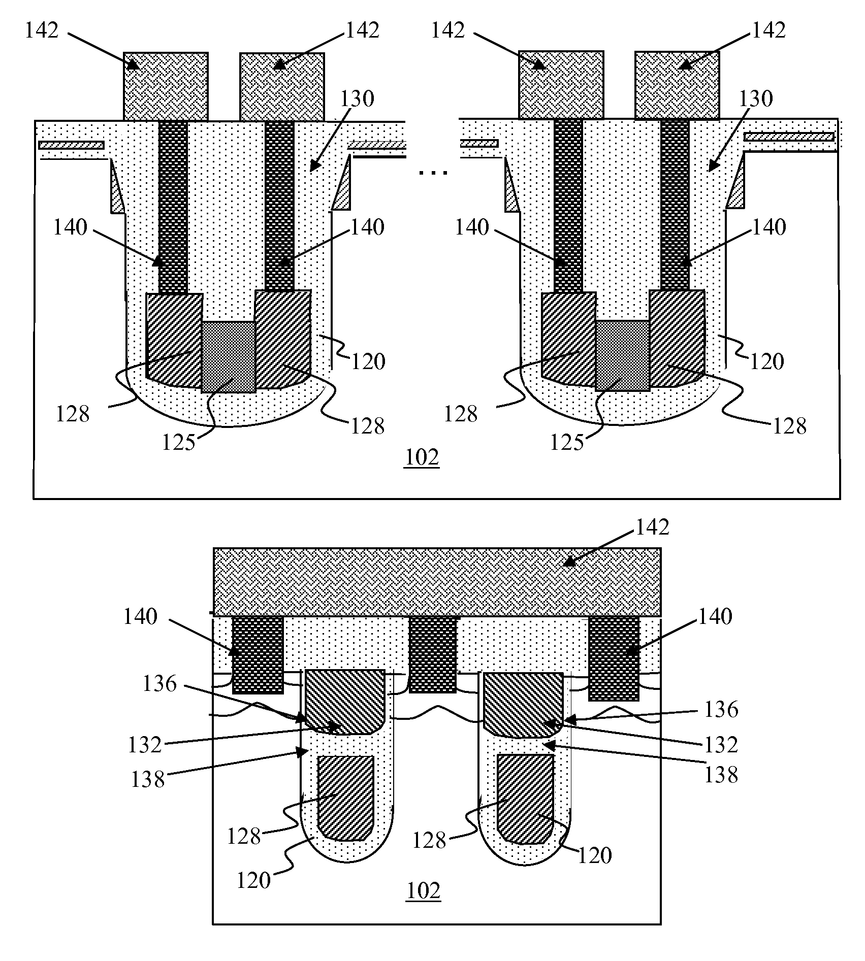
[0010]Embodiments of the present invention use the existing process flow for trench MOS and form electrostatic discharge (ESD) protection circuits inside the trench polysilicon (poly). Therefore, the ESD circuits are able to form without adding any extra mask layers. Such ESD can be formed for both SGT and normal trench MOSFET (i.e. a trench MOSFET without a shield electrode).

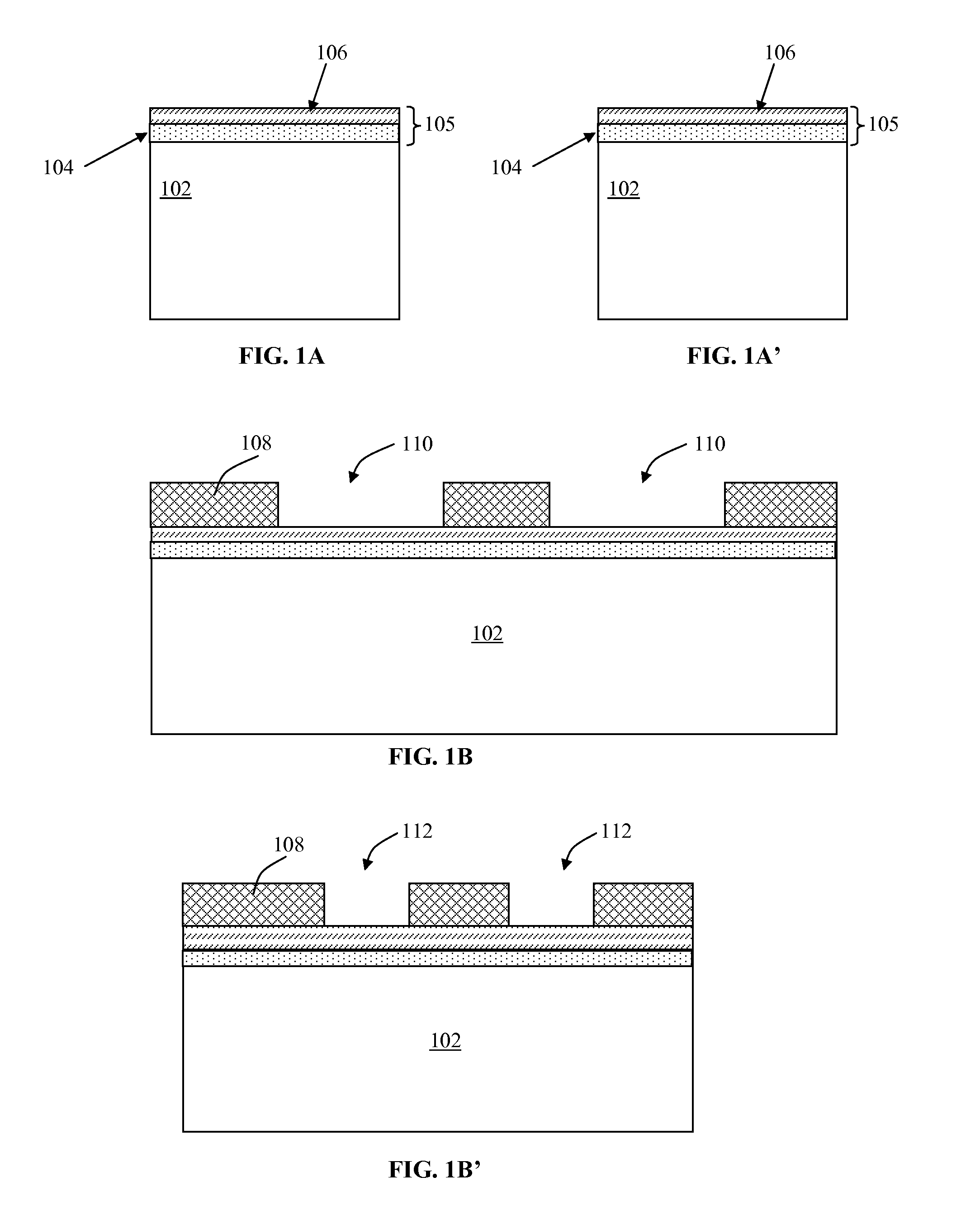
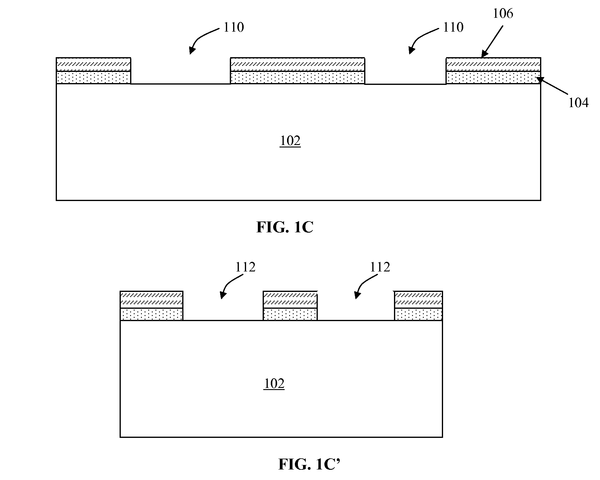
[0011]A fabrication process of the SGT trench MOSFET with integrated ESD circuit using only four masks is depicted in FIGS. 1A to 1L, and FIGS. 1A′ to 1L′. By way of ex...


PUM


Abstract

A semiconductor device and its method of fabrication are described. A trench formed in a semiconductor substrate is partially filling said trench with a semiconductor material that lines a bottom and sides of the trench, leaving a gap in a middle of the trench running lengthwise along the trench. A first portion of the semiconductor material located below the gap is doped with dopants of a first conductivity type. The gap is filled with a dielectric material. Second portions of the semiconductor material located on the sides of the trench on both sides of the dielectric material are doped with dopants of a second conductivity type. The doping forms a P-N-P or N-P-N structure running lengthwise along the trench with differently doped regions located side by side across a width of the trench.

Description

FIELD OF THE INVENTION[0001]This invention relates generally to the cell structure and device configuration of semiconductor devices. More particularly, this invention relates to an improved configuration for manufacturing an electrostatic discharge (ESD) protection circuit integrated with a semiconductor power device with reduced number of masks for Trench metal-oxide-semiconductor filed effect transistor (MOSFET) and Shield Gate Trench (SGT) MOSFET.BACKGROUND OF THE INVENTION[0002]Electrostatic discharge (ESD) is the sudden and momentary electric current that flows between two objects at different electrical potentials caused by direct contact or induced by an electrostatic field. ESD is a serious issue in solid state electronics, such as integrated circuits (IC) and power transistors made from semiconductor materials such as silicon and insulating materials such as silicon dioxide. Either of these materials can suffer permanent damage when subjected to high voltages; as a result,...

Claims


Application Information

Patent Timeline
Patent Type & Authority Patents(United States)
IPC IPC(8): H01L29/78H01L21/336
CPCH01L27/0259H01L29/7827H01L29/7393
Inventor CHANG, HONGCHEN, JOHN
Owner ALPHA & OMEGA SEMICON INC
Why Eureka
Try Eureka