CMOS having a SiC/SiGe alloy stack

a technology of sic/sige alloy and stack, which is applied in the direction of semiconductors, transistors, electrical devices, etc., can solve the problems of carbon-doped silicon oxide being more susceptible to wet etches, affecting the mobility of charge carriers (electrons) in the channel of the nfet, and affecting the efficiency of the

Active Publication Date: 2013-07-02
GLOBALFOUNDRIES US INC
View PDF24 Cites 26 Cited by
  • Summary
  • Abstract
  • Description
  • Claims
  • Application Information

AI Technical Summary

Problems solved by technology

However, addition of lanthanum degrades the mobility of charge carriers (electrons) in the channel of the NFET.
Thus, a significant undesirable side effect of degradation of charge carrier mobility accompanies the addition of lanthanum to alter the gate workfunction in an NFET.
Carbon-doped silicon oxide is more susceptible to wet etches or clean chemistries employed throughout semiconductor manufacturing sequences.
Particularly, the loss of the carbon-doped silicon oxide material in the shallow trench isolation structures during a reactive ion etch employed for gate patterning is significant, and results in a height variation of shallow trench isolation structures, pull-down of gate conductor materials, and electrical shorts of various semiconductor components through strips of residual gate conductor materials deposited in divots.
In addition, because the energy of ion implantation cannot be precisely controlled for shallow implantation, any carbon implanted structure has a thickness greater than 5 nm, making the carbon implantation method unusable for extremely thin semiconductor-on-insulator (ETSOI) structures in which the entire thickness of a top semiconductor layer is on the order of 5 nm.
Thus, use of carbon implantation to form carbon-doped silicon material is impractical for many applications.

Method used


Image

  • CMOS having a SiC/SiGe alloy stack
  • CMOS having a SiC/SiGe alloy stack
  • CMOS having a SiC/SiGe alloy stack

Examples


first embodiment

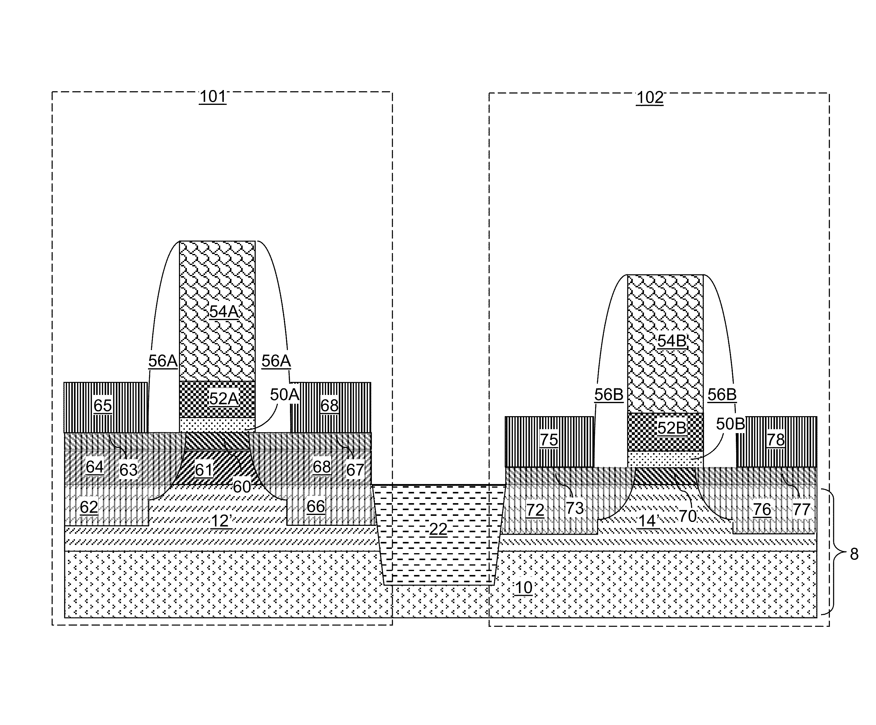
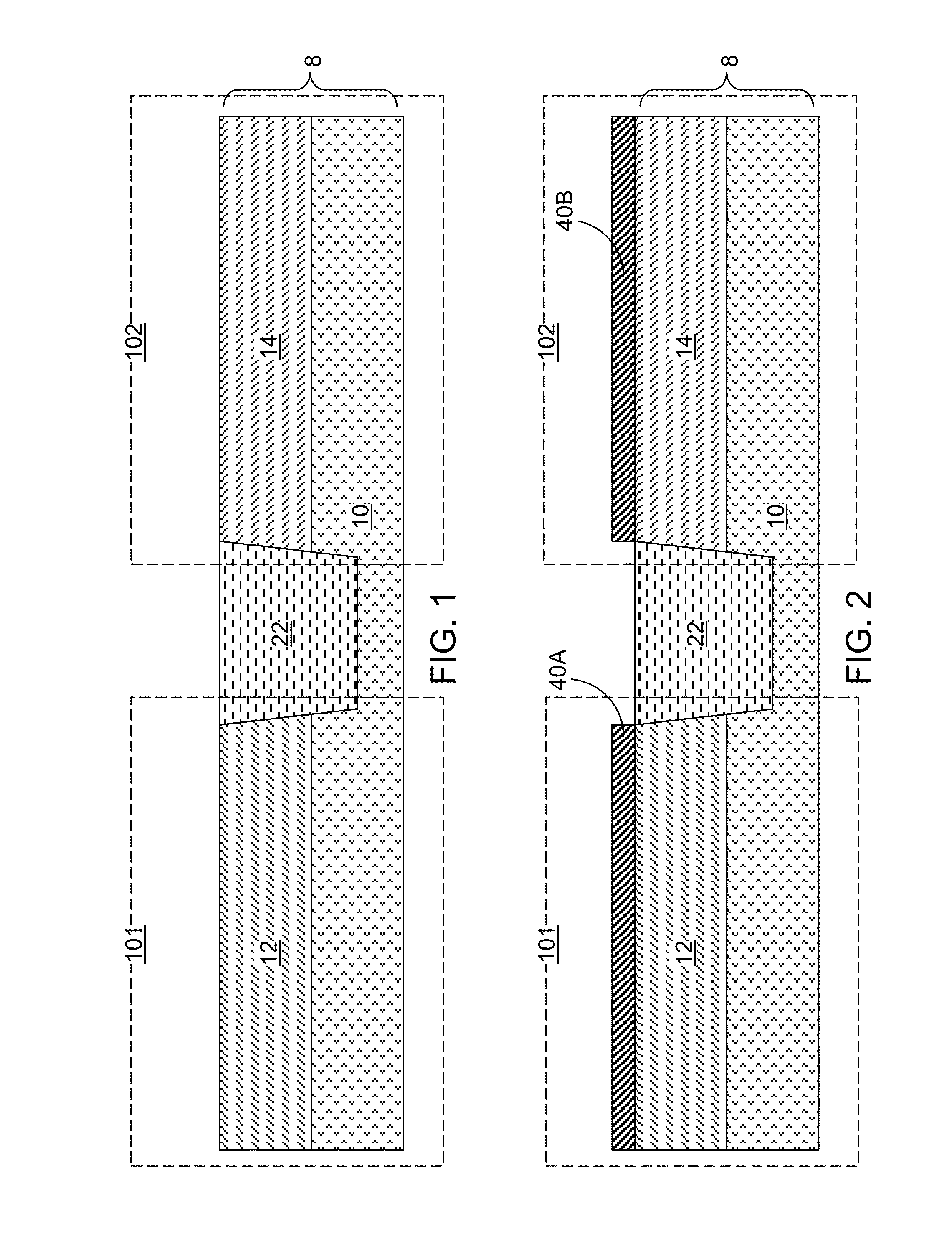
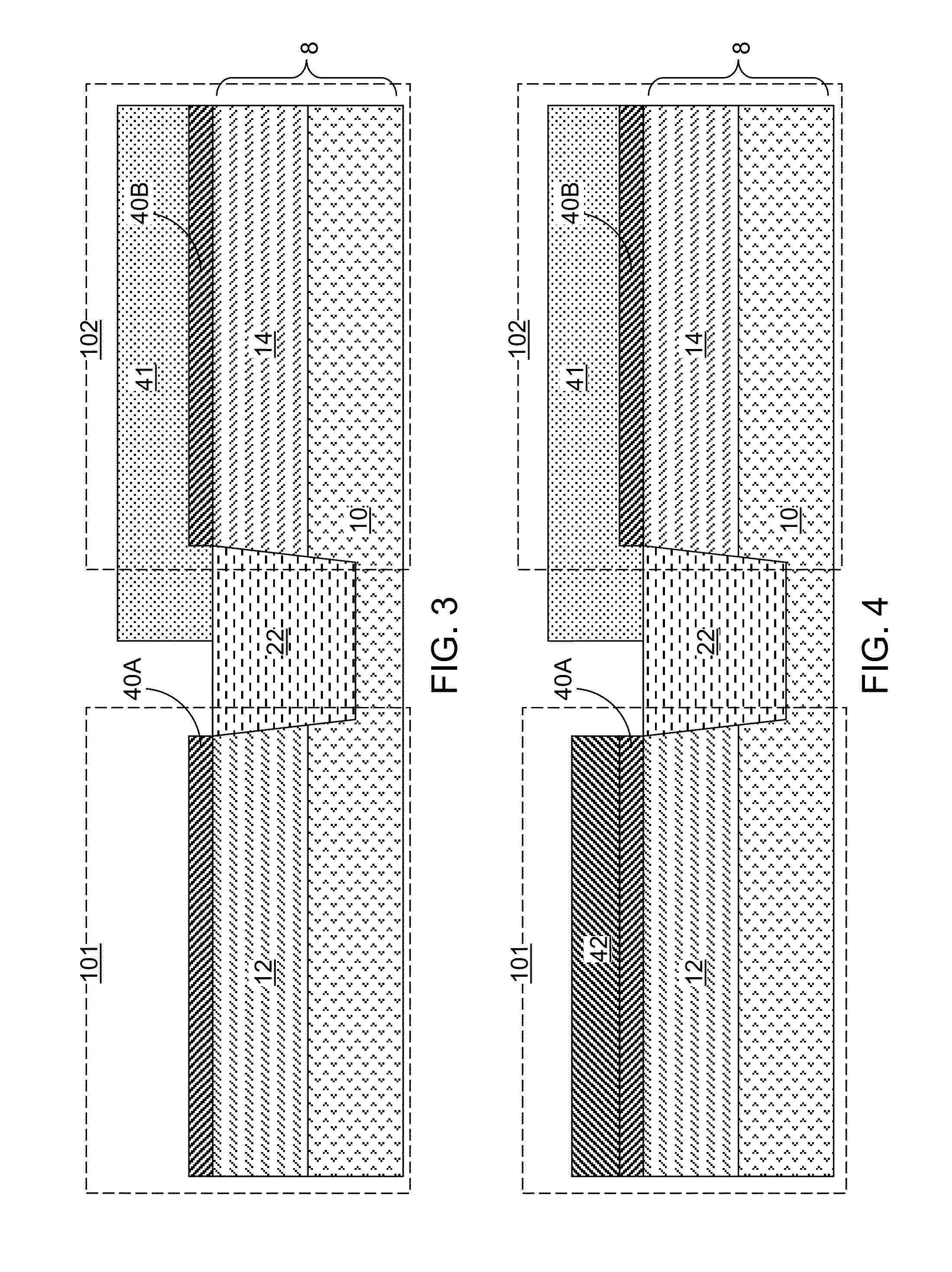
[0029]Referring to FIG. 1, a first exemplary semiconductor structure according to the present disclosure includes a substrate 8, which can be a bulk semiconductor substrate including at least one semiconductor material that contiguously extends from the topmost surface of the substrate 8 to a bottommost surface of the substrate 8. The substrate 8 includes a semiconductor material layer 10 having a semiconductor material. The semiconductor material of the semiconductor material layer 10 can be, for example, single crystalline silicon, a single crystalline silicon germanium alloy, or a single crystalline silicon carbon alloy.

[0030]An n-type well 12 including a silicon-containing semiconductor material and n-type dopants is formed in a region of the substrate 8, which is herein referred to as a p-type field effect transistor (PFET) region 101. The n-type well 12 can include n-doped single crystalline silicon. In one embodiment, the n-type well 12 can be formed by providing a single cry...

second embodiment

[0060]Referring to FIG. 7, a second exemplary semiconductor structure according to the present disclosure can be derived from the first exemplary semiconductor structures illustrated in FIGS. 1-6 by substituting a semiconductor-on-insulator (SOI) substrate 8′ for the substrate 8 in the first exemplary semiconductor structure. The SOI substrate as provided includes a handle substrate 110, a buried insulator layer 120, and a top silicon layer. The handle substrate 110 can include a semiconductor material, a conductive material, a dielectric material, or a combination thereof. The buried insulator layer 120 can be, for example, a layer of silicon oxide. The top silicon layer can be a single crystalline silicon layer. In one embodiment, the SOI substrate 8′ can be an extremely thin semiconductor-on-insulator substrate in which the thickness of the top silicon layer is not greater than 5 nm.

[0061]In the second embodiment, the n-type well 12 in the first embodiment is replaced with a firs...

sixth embodiment

[0094]Referring to FIG. 21, a sixth exemplary semiconductor structure according to the present disclosure can be derived from the fifth exemplary semiconductor structure of FIG. 13 by forming a dielectric masking layer 241 (See FIG. 15) and a silicon germanium alloy layer 242 (See FIG. 15) before forming silicon carbon alloy layers (240A, 240B; See FIG. 14).

[0095]The silicon germanium alloy layer 242 is deposited on the semiconductor surface of the first silicon fin 230A, while not being deposited on dielectric surfaces. The silicon germanium alloy material of the silicon germanium alloy layer 242 can be deposited by a selective deposition process, such as selective epitaxy, in which the silicon germanium alloy material nucleates, and is deposited, on semiconductor surfaces, while the silicon germanium alloy material does not nucleate, and is not deposited, on dielectric surfaces. The same deposition method can be employed to perform selective deposition of the silicon germanium all...


PUM

PropertyMeasurementUnit
thicknessaaaaaaaaaa
thicknessaaaaaaaaaa
thicknessesaaaaaaaaaa

Abstract

A delta doping of silicon by carbon is provided on silicon surfaces by depositing a silicon carbon alloy layer on silicon surfaces, which can be horizontal surfaces of a bulk silicon substrate, horizontal surfaces of a top silicon layer of a semiconductor-on-insulator substrate, or vertical surfaces of silicon fins. A p-type field effect transistor (PFET) region and an n-type field effect transistor (NFET) region can be differentiated by selectively depositing a silicon germanium alloy layer in the PFET region, and not in the NFET region. The silicon germanium alloy layer in the PFET region can overlie or underlie a silicon carbon alloy layer. A common material stack can be employed for gate dielectrics and gate electrodes for a PFET and an NFET. Each channel of the PFET and the NFET includes a silicon carbon alloy layer, and is differentiated by the presence or absence of a silicon germanium layer.

Description

BACKGROUND[0001]The present disclosure relates to semiconductor structures, and more particularly to planar and fin field effect transistor (FET) structures having a thin silicon carbon alloy layer in a channel, and methods of manufacturing the same.[0002]In some processing schemes for manufacturing complementary metal oxide semiconductor (CMOS) devices employing a high dielectric constant (high-k) gate dielectric material and a metallic gate electrode material, the gate workfunction of n-type field effect transistors (NFETs) is tuned by addition of lanthanum at a bottommost layer of a gate electrode, while the gate workfunction of p-type field effect transistors (PFETs) is determined by the material composition of the gate electrode that does not include added lanthanum. The greater the amount of lanthanum that is added to a gate electrode of an NFET, the greater the shift of the gate workfunction to the valence band edge of silicon. However, addition of lanthanum degrades the mobi...

Claims


Application Information

Patent Timeline
Patent Type & Authority Patents(United States)
IPC IPC(8): H01L29/76H01L31/062H01L31/113H01L29/94H01L31/119H01L27/01H01L27/12H01L31/0392
CPCH01L21/8238H01L21/84H01L29/1054H01L21/823807H01L29/66651H01L27/1203
Inventor CHIDAMBARRAO, DURESETIGREENE, BRIAN J.LIANG, YUEYU, XIAOJUN
Owner GLOBALFOUNDRIES US INC
Why Eureka
Try Eureka