
Decoupling capacitor insertion using hypergraph connectivity analysis

a hypergraph connectivity and capacitor technology, applied in the direction of instruments, computing, electric digital data processing, etc., can solve the problems of large number of cells, difficult physical design without the aid of computers, and complicated connections between cells

Active Publication Date: 2013-07-02
GLOBALFOUNDRIES US INC
View PDF7 Cites 20 Cited by
  • Summary
  • Abstract
  • Description
  • Claims
  • Application Information

AI Technical Summary

Benefits of technology

The present invention provides an improved method for placing decoupling capacitors (dcaps) in an integrated circuit design. This method accurately places dcaps near critical logic, and allows designers to control the location of dcaps for specific logic. This helps to improve the overall performance and efficiency of the integrated circuit design.

Problems solved by technology

An IC may include a very large number of cells and require complicated connections between the cells.
Due to the large number of components and the details required by the fabrication process for very large scale integrated (VLSI) devices such as microprocessors and application-specific integrated circuits (ASICs), physical design is not practical without the aid of computers.
One problem that has arisen in these modern electronic devices relates to noise in the power grid of the device.
Substantial noise is generated in an integrated circuit chip as digital electronic functions are interconnected or decoupled.
The power grid provides the power and ground signals throughout the chip, and these are among the most important signals to control reliably, since supply voltage variations can lead not only to problems related to spurious transitions in some cases (particularly when dynamic logic is used), but also to delay variations and timing unpredictability.
Even if a reliable supply is provided at an input pin of a chip, it can deteriorate significantly within the chip due to imperfections in the conductors that transmit these signals throughout the chip.
Noise in modern electronic circuits is particularly troublesome as it increases the requirements on the noise margins and other circuit parameters.
Noise margins have been greatly reduced in modern designs due to the lowering of supply voltages and the presence of a larger number of potential noise generators.
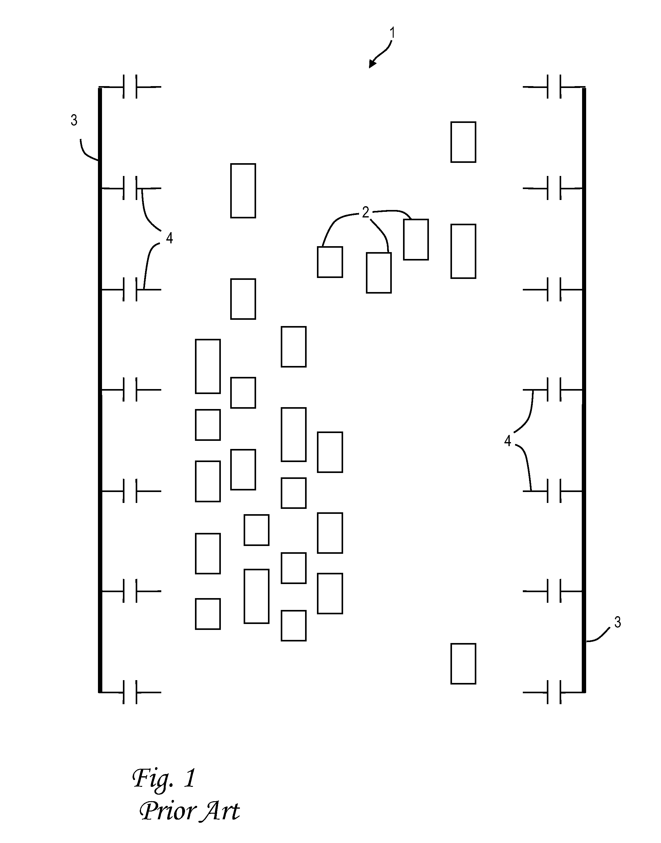
The problem with this approach is that the resulting dcap placement is not necessarily ideal based on the locations of the logic gates, and can negatively impact overall placement results such as timing.
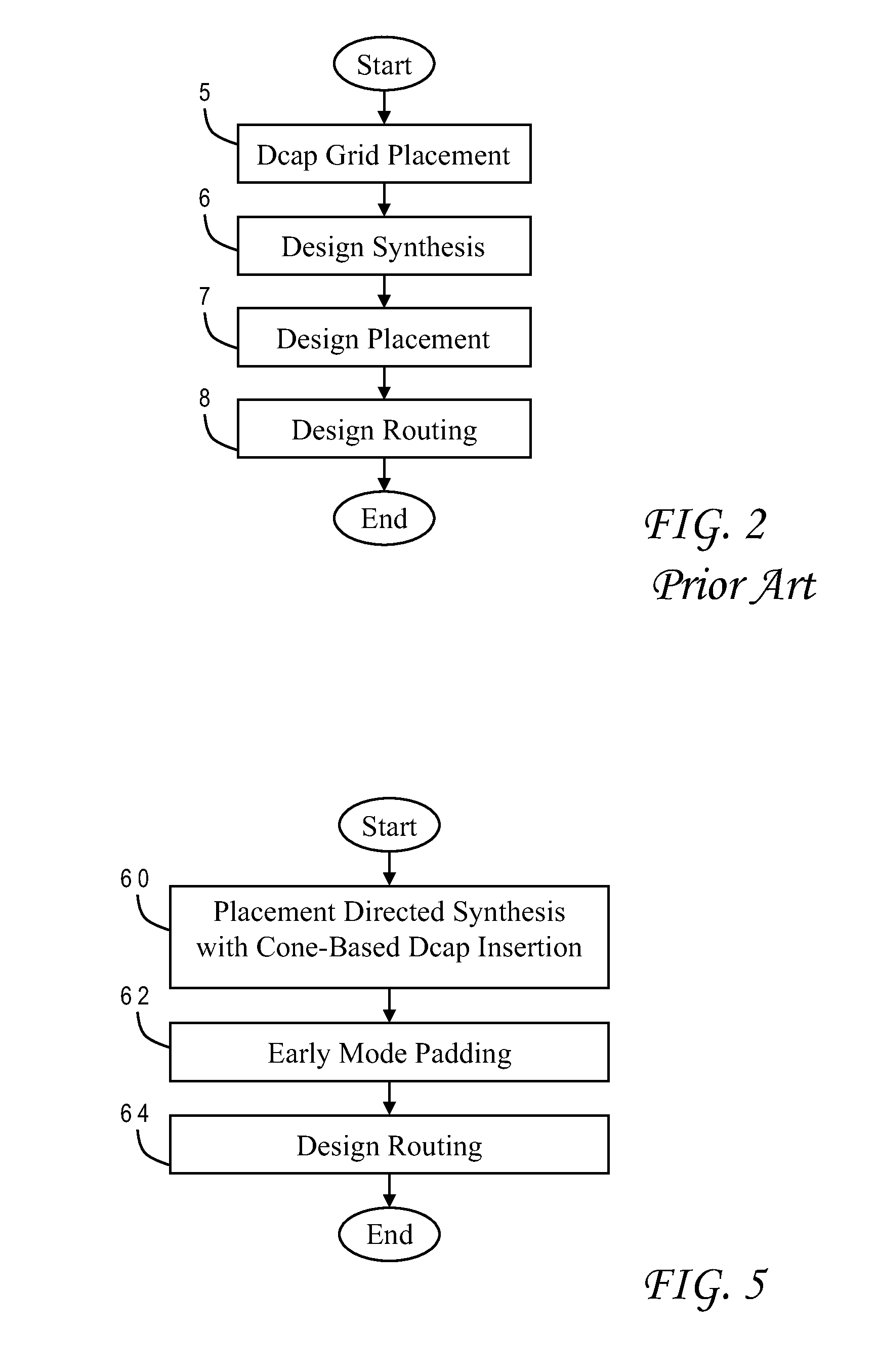
It is impossible to optimize dcap placement in this process since the dcaps are all inserted prior to placement of the circuit elements in the geometric layout.
Dcaps can then be inserted at those areas, but this ad hoc approach severely limits placement to available locations.
This approach is also manually intensive.

Method used


Image

  • Decoupling capacitor insertion using hypergraph connectivity analysis
  • Decoupling capacitor insertion using hypergraph connectivity analysis
  • Decoupling capacitor insertion using hypergraph connectivity analysis

Examples


Embodiment Construction

)

[0030]With reference now to the figures, and in particular with reference to FIG. 3, there is depicted one embodiment 10 of a computer system in which the present invention may be implemented to carry out the design of an integrated circuit. Computer system 10 is a symmetric multiprocessor (SMP) system having a plurality of processors 12a, 12b connected to a system bus 14. System bus 14 is further connected to a combined memory controller / host bridge (MC / HB) 16 which provides an interface to system memory 18. System memory 18 may be a local memory device or alternatively may include a plurality of distributed memory devices, preferably dynamic random-access memory (DRAM). There may be additional structures in the memory hierarchy which are not depicted, such as on-board (L1) and second-level (L2) or third-level (L3) caches.

[0031]MC / HB 16 also has an interface to peripheral component interconnect (PCI) Express links 20a, 20b, 20c. Each PCI Express (PCIe) link 20a, 20b is connected t...


PUM


Abstract

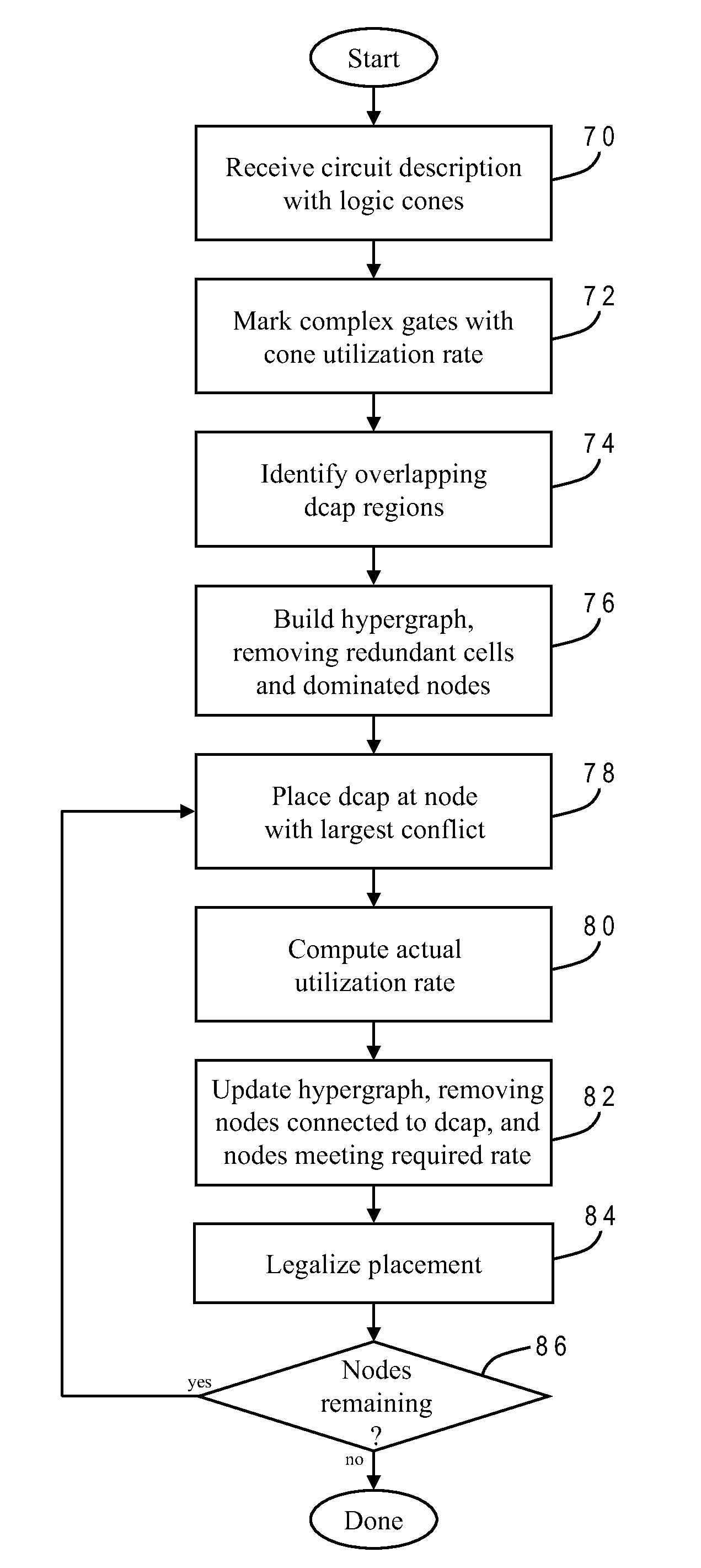
Decoupling capacitors (dcaps) are placed in an IC design by assigning different dcap utilization rates to logic cones, applying the rates to corresponding dcap regions surrounding cells in the cones, identifying any overlap of regions from different logic cones, and inserting a dcap at the overlapping region having the highest dcap utilization rate. The best location for the dcap is computed using a hypergraph wherein the cells are edges and the regions are nodes. Any node that is dominated by another node is removed and its edge is extended to the dominating node. The dcap is inserted in the region having the most edges (the edges can be weighted). The process is repeated iteratively, updating the hypergraph by removing nodes connected to dcap location, and inserting the next dcap at a region corresponding to the node which then has the greatest number of connected edges.

Description

BACKGROUND OF THE INVENTION[0001]1. Field of the Invention[0002]The present invention generally relates to the design of semiconductor chips and integrated circuits, and more particularly to a method of inserting decoupling capacitors in an integrated circuit design.[0003]2. Description of the Related Art[0004]Integrated circuits are used for a wide variety of electronic applications, from simple devices such as wristwatches, to the most complex computer systems. A microelectronic integrated circuit (IC) chip can be thought of as a collection of logic cells with electrical interconnections between the cells, formed on a semiconductor substrate (e.g., silicon). An IC may include a very large number of cells and require complicated connections between the cells. A cell is a group of one or more circuit elements such as transistors, capacitors, resistors, inductors, and other basic circuit elements combined to perform a logic function. Cell types include, for example, core cells, scan ...

Claims


Application Information

Patent Timeline
Patent Type & Authority Patents(United States)
IPC IPC(8): G06F17/50
CPCG06F17/5063G06F17/5072G06F2217/78G06F30/36G06F30/392G06F2119/06G06F30/373
Inventor HOPKINS, JEREMY T.PAPA, DAVID A.WARD, SAMUEL I.
Owner GLOBALFOUNDRIES US INC
Learn More