Organic semiconductor compound, semiconductor element, solar battery, and process for producing organic semiconductor compound

a technology of organic semiconductors and semiconductor elements, applied in the field of organic semiconductor compounds, can solve the problems of inability to maintain high performance or stability in the processing mode of thin films, and the development of organic semiconductors such as organic amorphous semiconductors and the like is remarkably delayed

Inactive Publication Date: 2013-08-06
NAT INST FOR MATERIALS SCI
View PDF9 Cites 0 Cited by
  • Summary
  • Abstract
  • Description
  • Claims
  • Application Information

AI Technical Summary

Benefits of technology

[0051]According to the present invention, there can be obtained a compound or the like that can become a material in which many functions are controllable.
[0052]Still other objects, features or advantages of the present invention will become clear by the detailed description based on exemplified embodiments and attached drawings of the present invention, which will be described later.

Problems solved by technology

However, with respect mainly to the semiconductor portion, crystal or doped polymer is the mainstream and even when taking a consideration globally, the current situation is in that the development of organic semiconductors such as an organic amorphous semiconductor and the like are remarkably delayed.
Also, there are presently promoted developments of an organic thin film solar cell and an organic EL (Organic Electro-Luminescence) device, which use a low molecule it compound and a photoconductivity-doped polymer, but it is well known that the performances thereof are worse compared with that of an inorganic Si-based amorphous solid.
This is related to a fact that high performance or stability cannot be maintained in the processing mode of a thin film, a chip or the like.
That is because the devices known as organic amorphous solids are limited to similar it electronic system starburst molecule groups in which there exist devices expressing conductivity on the radical bodies thereof, but the value thereof is generally very low.
Further, a general organic conductor of a charge transfer type is produced by an electrolysis method or the like, so that it is difficult to control molecular arrangement.
Also, the electronic material property is largely dependent on the crystal structure, so that there is difficulty also in a viewpoint of the application to the thin film by polymerization and liquid crystallization which are needed for industrialization.
Also, for the conductive polymer which is made to be a semiconductor by executing a doping, it is difficult to control the arrangement thereof, so that it is difficult for the charge separation capability to be improved.
Also, it lacks in chemical stability and the time degradation thereof is terrific.
InSc and GaAs crystals which have high Hall effect are rare metals and therefore, they are expensive and also lack in workability.

Method used


Image

  • Organic semiconductor compound, semiconductor element, solar battery, and process for producing organic semiconductor compound
  • Organic semiconductor compound, semiconductor element, solar battery, and process for producing organic semiconductor compound
  • Organic semiconductor compound, semiconductor element, solar battery, and process for producing organic semiconductor compound

Examples


Embodiment Construction

[0074]Hereinafter, it will be explained with respect to exemplified embodiments of the present invention in detail while referring to drawings.

[Brief Summary]

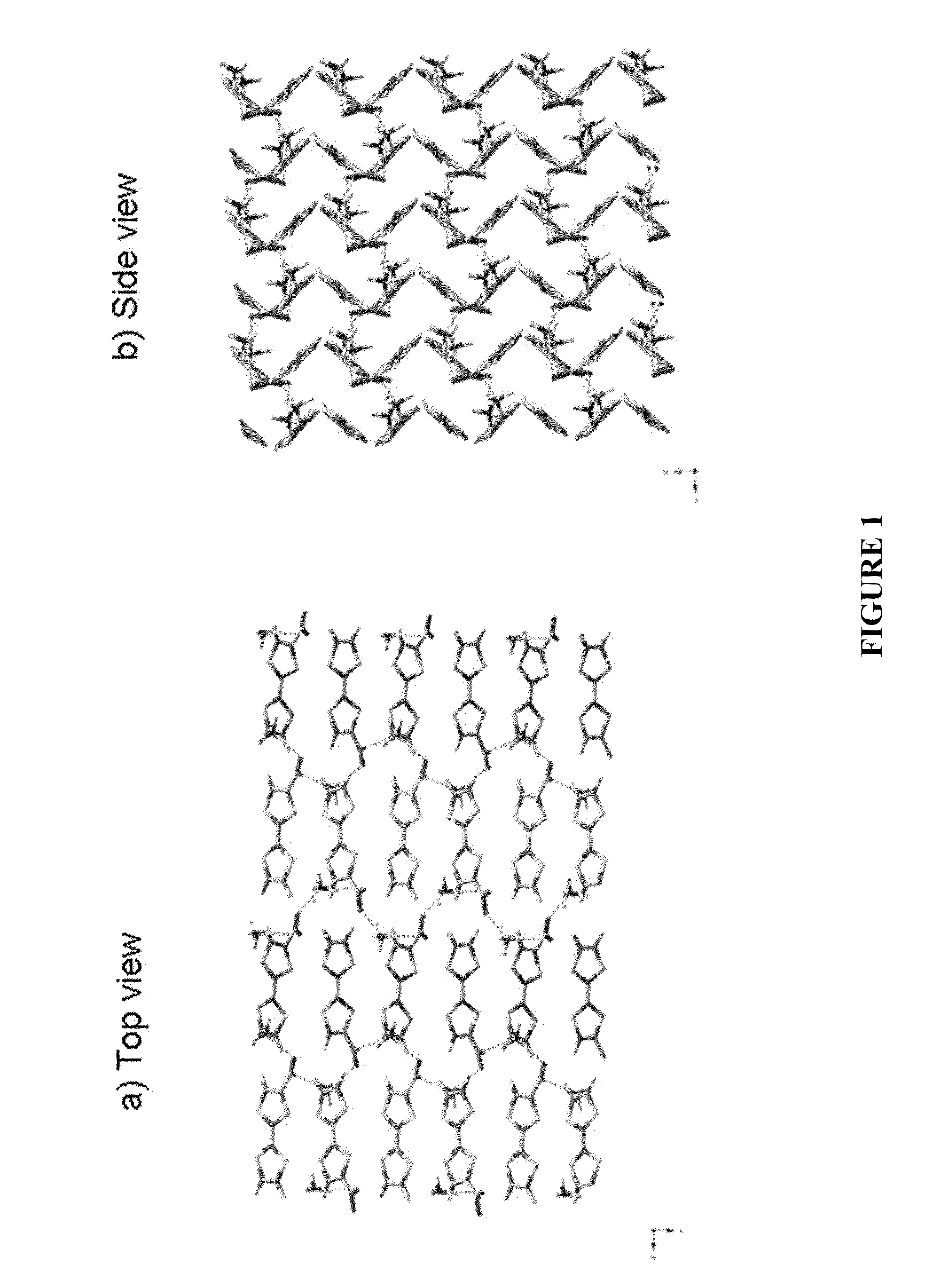
[0075]As a result of day-to-day bona fide researches of the present inventors, it was proved that an organic semiconductor can be obtained by a simple technique such as to salt-form a donor molecule with an inorganic acid or an inorganic base. There is a prospect that a variety of organic semiconductors can be produced by similar techniques and this technique is an epoch-making technique. Here, two examples are briefly shown as illustrative embodiments thereof.[0076]1) A tetrathiafulvalene-2-carboxylic acid was obtained by total yield 65% from tetrathiafulvalene (TTF) through two processes and thereafter, the salt was prepared by a 28% aqueous ammonia solution and a 1:1 ammonium tetrathiafulvalene-2-carboxylic acid salt which is pure at the element analysis level was obtained.

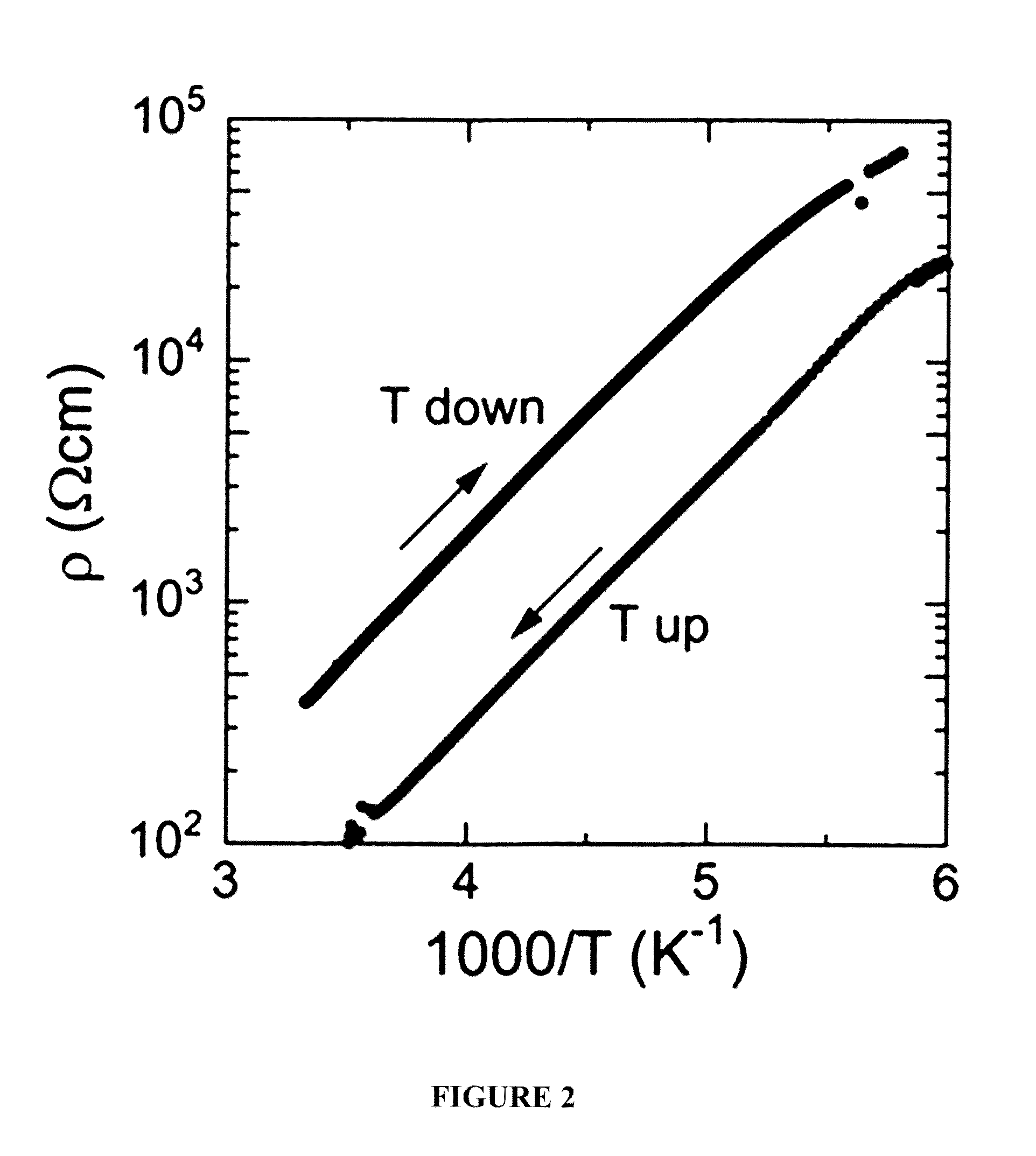
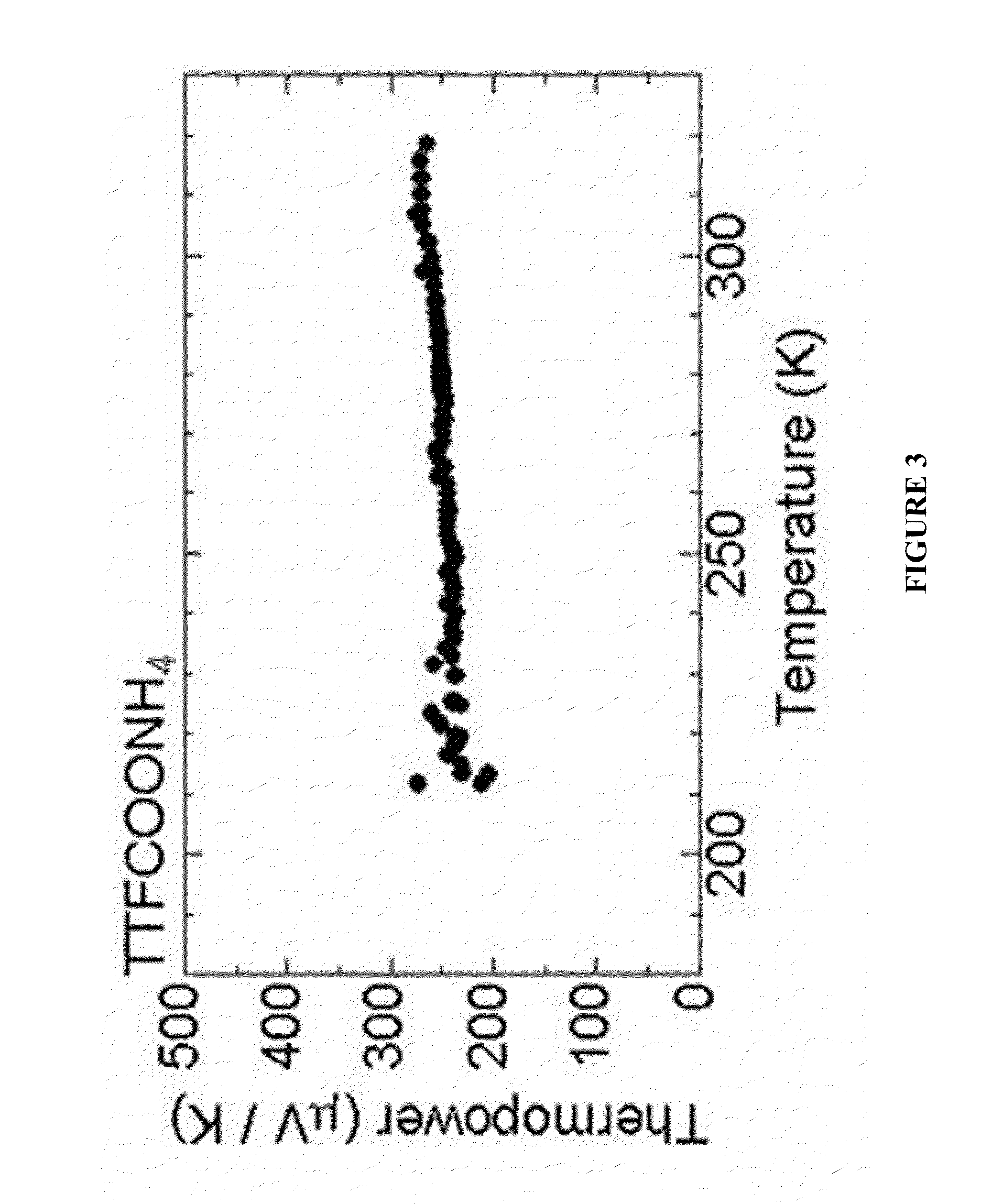
[0077]Electrical conductivity when pelletizing the o...


PUM

PropertyMeasurementUnit
electrical conductivityaaaaaaaaaa
Electrical conductivityaaaaaaaaaa
thicknessaaaaaaaaaa

Abstract

Disclosed is, for example, a compound that can be a material which can control many functions. According to a first aspect of the present invention, there is provided an organic semiconductor compound characterized in that the organic semiconductor compound is produced by forming a salt of organic molecules as a donor with an inorganic acid or an inorganic base and causes self-accumulation. According to the above constitution, the organic semiconductor compound can be obtained in a simple manner. According to a second aspect of the present invention, there is provided an organic compound characterized by being produced by deriving an ammonia salt or a hydroxyamine salt from a compound having a tetrathiafulvalene analogue site in the skeleton thereof and containing a protonic acid functional group. According to the above constitution, an organic compound which can control many functions can be obtained.

Description

TECHNICAL FIELD[0001]The present invention relates to an organic compound and particularly to an organic semiconductor compound, a semiconductor device, a solar cell and a producing method of an organic semiconductor compound.BACKGROUND ART[0002]Si-based amorphous semiconductors occupy the majority of the market presently due to the excellent workability thereof. For example, there is used an Si-based amorphous semiconductor frequently for a TFT (Thin Film Transistor) of a liquid crystal display or for a solar cell.[0003]On the other hand, it is expected for the organic semiconductor to be applied to a wearable device because of such characteristics referred to as lightweight and flexibility. However, with respect mainly to the semiconductor portion, crystal or doped polymer is the mainstream and even when taking a consideration globally, the current situation is in that the development of organic semiconductors such as an organic amorphous semiconductor and the like are remarkably ...

Claims


Application Information

Patent Timeline
Patent Type & Authority Patents(United States)
IPC IPC(8): A61K31/385C07D339/06
CPCC07D339/06H01L51/0068C07C391/00H01L51/0074Y02E10/549H01L51/4293Y02P70/50H10K85/655H10K30/40H10K85/6576
Inventor SAIGO, KAZUHIKOKOBAYASHI, YUKA
Owner NAT INST FOR MATERIALS SCI
Why Eureka
Try Eureka