Nanoelectric memristor device with dilute magnetic semiconductors

a technology of dilute magnetic semiconductors and memristor devices, which is applied in semiconductor devices, digital storage, instruments, etc., can solve the problems of difficult design of large-scale integration memory devices for low-power applications using this technology, the switching speed is much slower in memristor devices when switching, and the conductance in both on/off states

Inactive Publication Date: 2013-08-06
UNIVERSITY OF TOLEDO
View PDF18 Cites 50 Cited by
  • Summary
  • Abstract
  • Description
  • Claims
  • Application Information

AI Technical Summary

Problems solved by technology

However, current memristor devices, such as the one shown in FIG. 1 offer a relatively low ON / OFF conductance ratio, making it difficult to design large scale integration memory devices for low power applications using this technology.
Additionally, the switching speed is much slower in memristor devices when compared with other memory technologies (such as SRAM and DRAM devices).
In the same fashion, having high conductance in both ON / OFF states consumes considerable current to be used in order to read the stored data.
This can present a power consumption problem that can restrict memristor technologies for use in low power devices.

Method used


Image

  • Nanoelectric memristor device with dilute magnetic semiconductors
  • Nanoelectric memristor device with dilute magnetic semiconductors
  • Nanoelectric memristor device with dilute magnetic semiconductors

Examples


Embodiment Construction

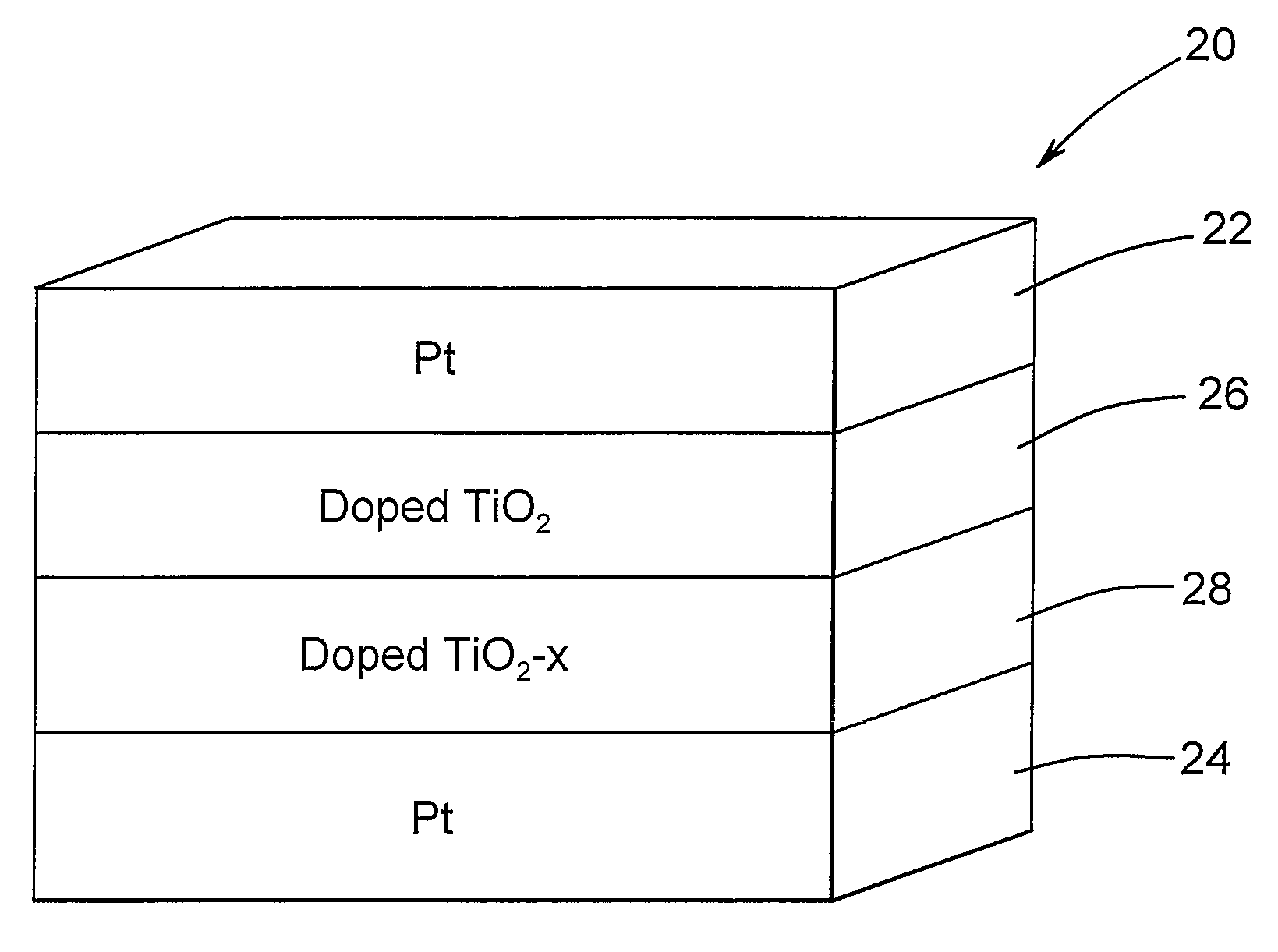
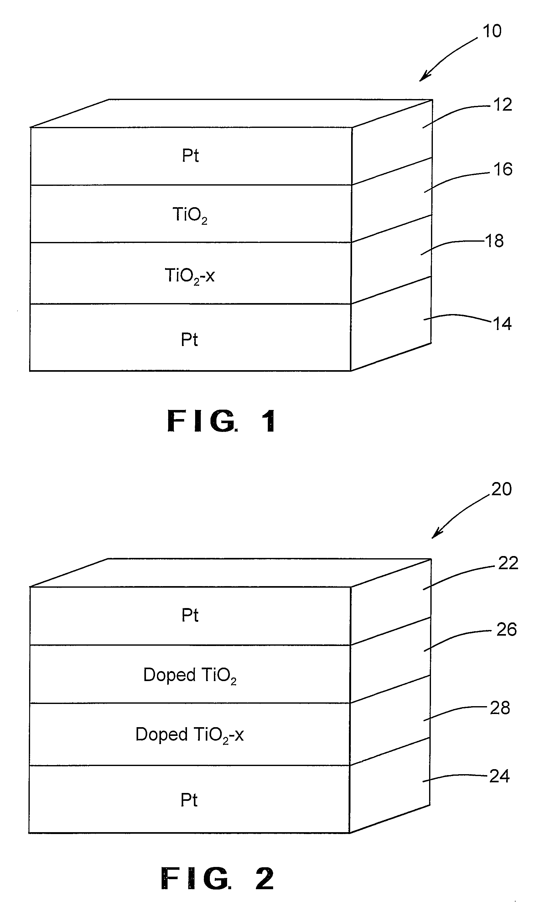
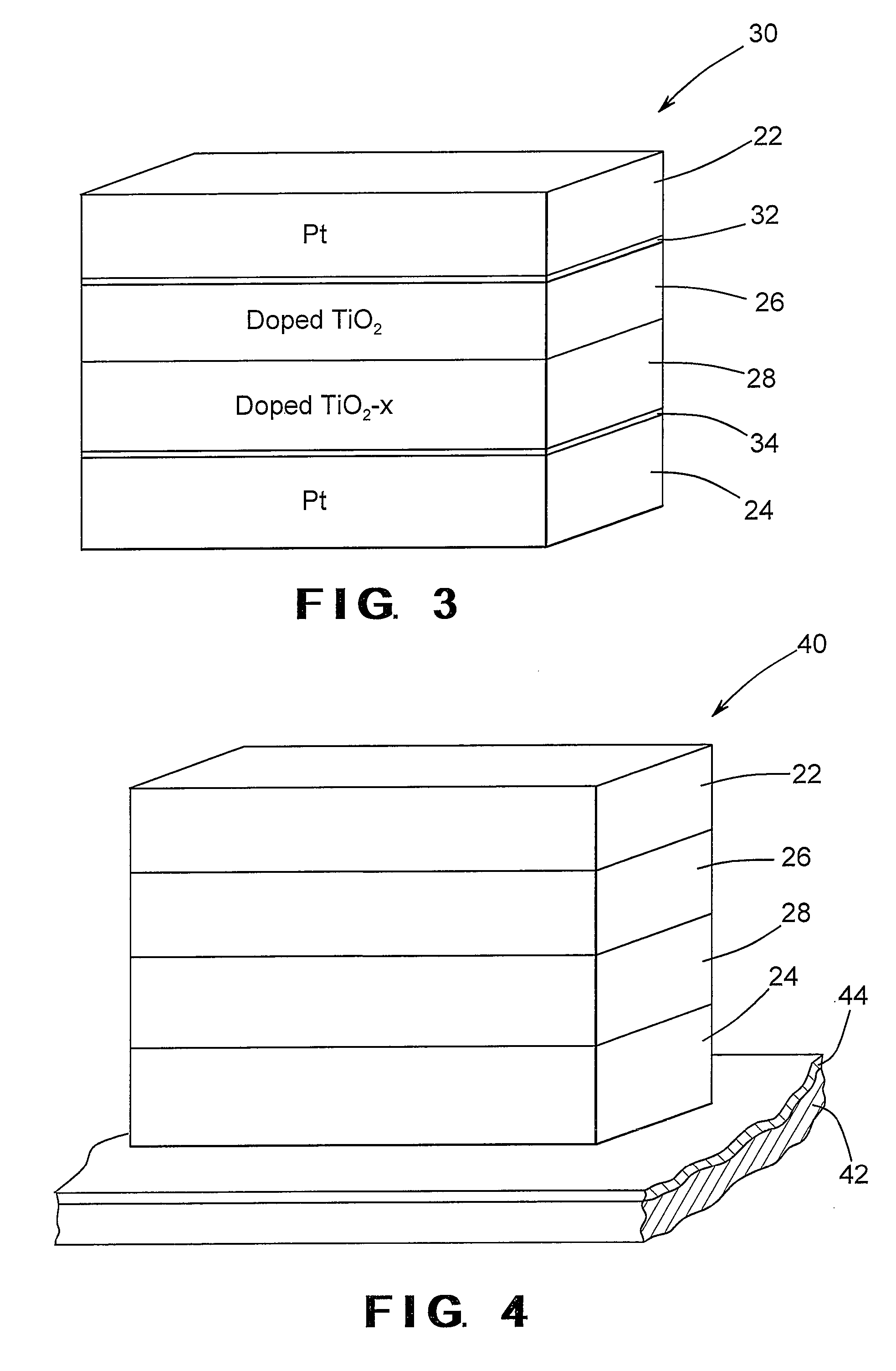
[0021]As described herein, a magnetic and / or a paramagnetic doping material (such as, for example, manganese, cobalt, iron, nickel, or chromium) is added to one or both of transition metal oxide layers of a nanoelectronic memristor device. The transition metal oxide layers may, for example, be formed from titanium dioxide, hafnium dioxide, strontium titanium oxide, zirconium dioxide, zinc oxide, tantalum oxide, hafnium lanthanum oxide, or hafnium aluminum oxide. The doping with the magnetic and / or a paramagnetic doping material achieves the formation of a dilute magnetic semiconductor oxide material, where change in magnetization can be achieved as a function of the oxygen vacancies concentration in the magnetically doped layer. Under an applied bias, the oxygen-vacancies can be injected from vacancy-rich metal oxide into the oxygen-rich / stochiometric metal oxide. This changes the oxygen vacancy concentration in the magnetic metal doped layer and, thus, results in the change in the ...


PUM

PropertyMeasurementUnit
thicknessaaaaaaaaaa
temperatureaaaaaaaaaa
pressureaaaaaaaaaa

Abstract

A nanoelectric memristor device includes a first electrode and a layer of oxygen-vacancy-rich metal oxide deposited upon a surface of the first electrode. A layer of oxygen-rich / stochiometric metal oxide is deposited upon a surface of the oxygen-vacancy-rich metal oxide layer that is opposite from said first electrode. At least one of the oxygen-vacancy-rich metal oxide and oxygen-rich / stochiometric metal oxide layers is doped with one of a magnetic and a paramagnetic material. A second electrode is adjacent to a surface of the oxygen-rich / stochiometric metal oxide layer that is opposite from the oxygen-rich / stochiometric metal oxide layer.

Description

[0001]This application claims the benefit of U.S. Provisional Application No. 61 / 414,572, filed Nov. 17, 2010, the disclosure of which is incorporated herein by reference.STATEMENT REGARDING FEDERALLY SPONSORED RESEARCH OR DEVELOPMENT[0002]Not applicable.BACKGROUND OF THE INVENTION[0003]This invention relates in general to electronic nonvolatile memory devices and in particular to nanoelectronic memristor devices.[0004]The logic and memory device market has generally been following Moore's Law for the last three decades by greatly increasing the number of components that can be provided on an integrated circuit chip. One apparent impact of this densification of solid state electronic components on a chip can be seen in consumer electronic products market, where there has been a large increase in the functionality of consumer electronic products such as, for example, cell phones, gaming consoles, iPhones, and other all-in-one devices, in recent years. In the area of high performance ...

Claims


Application Information

Patent Timeline
Patent Type & Authority Patents(United States)
IPC IPC(8): H01L29/00
CPCH01L45/08H01L45/1233H01L45/146H01L45/1625H01L45/1658G11C11/16H10N70/24H10N70/026H10N70/046H10N70/826H10N70/8833
Inventor JHA, RASHMIORDOSGOITTI, JORHANLONG, BRANDEN
Owner UNIVERSITY OF TOLEDO
Why Eureka
Try Eureka