Method for lift-off of light-emitting diode substrate

a technology of light-emitting diodes and substrates, which is applied in the direction of basic electric elements, electrical equipment, semiconductor devices, etc., can solve the problems of low heat dissipation efficiency, current crowding, and production cost and luminous efficiency

Active Publication Date: 2013-08-13
QUANZHOU SANAN SEMICON TECH CO LTD
View PDF14 Cites 23 Cited by
  • Summary
  • Abstract
  • Description
  • Claims
  • Application Information

AI Technical Summary

Benefits of technology

[0015]The method according to an embodiment of the present invention may bring the following advantageous effects. The dislocation density in the growth of a GaN-based epitaxial layer can be effectively reduced; lattice quality can be improved without any internal damage to the GaN film; performance of the photoelectric device can be elevated; and luminous efficiency can be improved.
. The dislocation density in the growth of a GaN-based epitaxial layer can be effectively reduced; lattice quality can be improved without any internal damage to the GaN film; performance of the photoelectric device can be elevated; and luminous efficiency can be improved.

Problems solved by technology

However, for the popularization of semiconductor lighting, a number of problems are still left to be solved, among which the most important one lies in production cost and luminous efficiency.
A high-power GaN-based LED with a lateral structure in which sapphire is used as a growth substrate has the disadvantages including low heat dissipation efficiency, current crowding, low current density and high production cost.
However, the processing steps of flip chip are complex and the production cost is high.
However, this approach has the following problems: (1) laser lift-off may crack the GaN film internally, causing electrical leakage; (2) the heat generated in the process of laser lift-off of a sapphire substrate is high, since the wafer bonding layer is just several micrometers away from the interface between the sapphire substrate and GaN, the bonding layer is likely to be affected (e.g., remelt); and (3) the laser lift-off techniques are not compatible with earlier processing processes, and the machines and tools are costly.

Method used


Image

  • Method for lift-off of light-emitting diode substrate
  • Method for lift-off of light-emitting diode substrate
  • Method for lift-off of light-emitting diode substrate

Examples


Embodiment Construction

[0027]The present invention will be described hereinafter in detail in conjunction with the embodiments.

[0028]The present invention will be described hereinafter in detail in conjunction with the accompanying drawings and the embodiments.

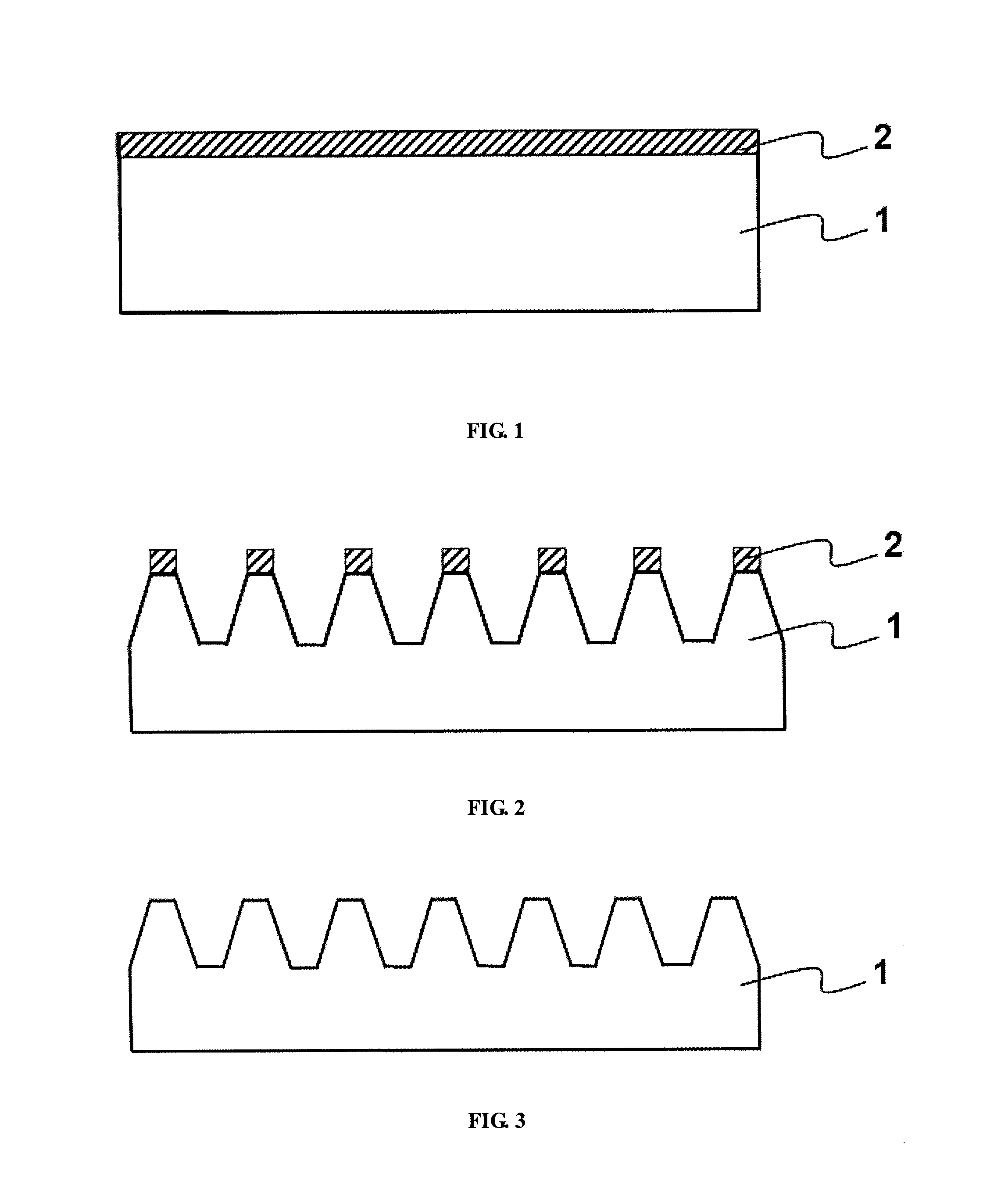
[0029]As shown in FIG. 1, a SiO2 transitional layer 2 is deposited on a sapphire substrate 1.

[0030]As shown in FIG. 2, a patterned SiO2 transitional layer 2 with periodically distributed rectangular patterns is formed by masking and etching.

[0031]As shown in FIG. 3, a transitional layer is removed so as to form a patterned sapphire substrate 1.

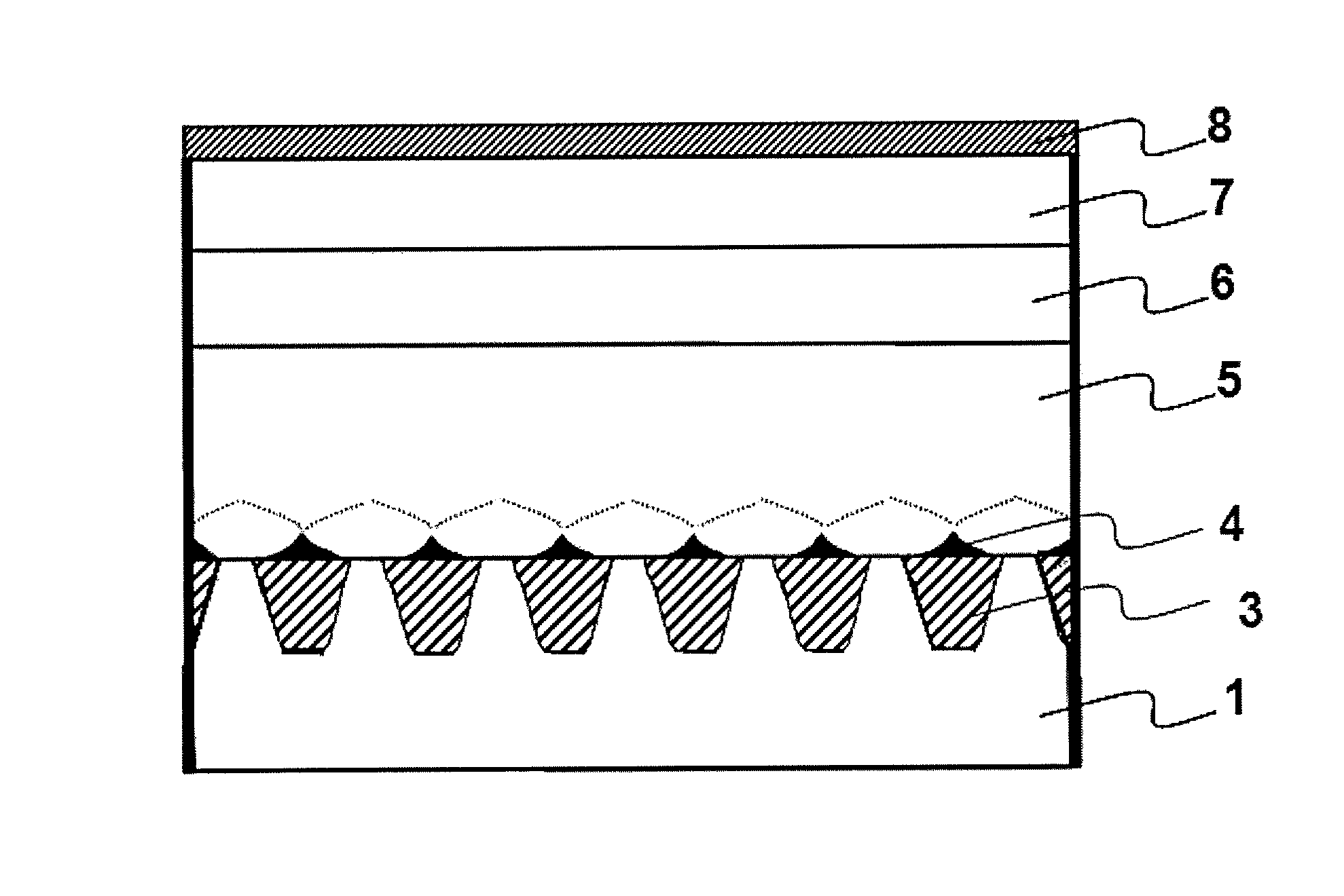
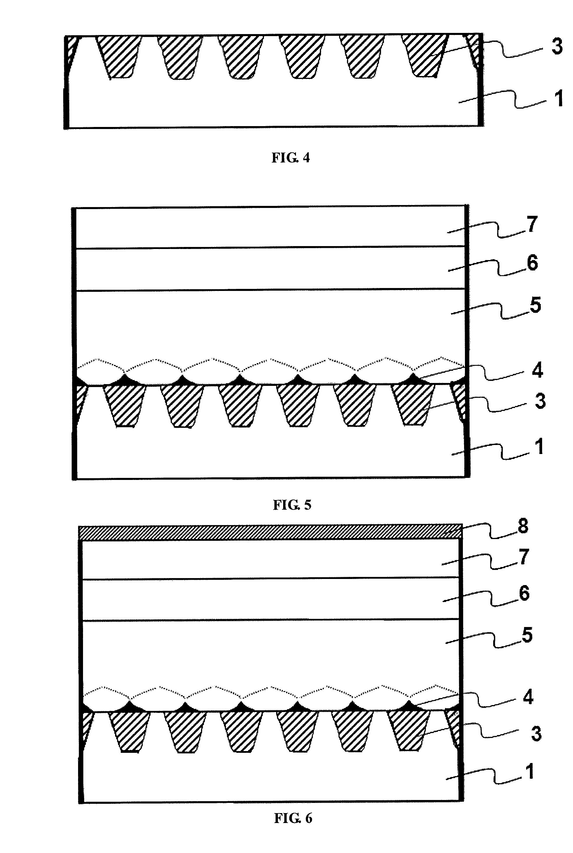
[0032]As shown in FIG. 4, a SiO2 blocking layer 3 is formed on the sapphire substrate, and chemical-mechanical polishing is performed on the SiO2 blocking layer 3 so that the surface of the SiO2 blocking layer 3 is flush with surfaces of projections of the patterned sapphire substrate 1.

[0033]As shown in FIG. 5, a GaN epitaxial layer is grown on the patterned sapphire substrate 1, cavity structures 4 are forme...


PUM

PropertyMeasurementUnit
electroluminescenceaaaaaaaaaa
brightnessaaaaaaaaaa
luminous efficiencyaaaaaaaaaa

Abstract

The present invention discloses a method for lift-off of an LED substrate. By eroding the sidewall of a GaN epitaxial layer, cavity structures are formed, which may act in cooperation with a non-fully filled patterned sapphire substrate from epitaxial growth to cause the GaN epitaxial layer to separate from the sapphire substrate. The method according to an embodiment of the present invention can effectively reduce the dislocation density in the growth of a GaN-based epitaxial layer; improve lattice quality, and realize rapid lift-off of an LED substrate, and has the advantages including low cost, no internal damage to the GaN film, elevated performance of the photoelectric device and improved luminous efficiency.

Description

[0001]The present application claims the benefit of Chinese patent application No. 201110024096.1 titled “Method for Lift-off of Light-Emitting Diode Substrate” and filed with the State Intellectual Property Office on Jan. 21, 2011, which is incorporated herein by reference in its entirety.FIELD OF THE INVENTION[0002]The present invention relates to a method for lift-off of a light-emitting diode (LED) substrate, and in particular to a non-laser based method for lift-off of a sapphire substrate used in the manufacturing of a gallium nitride (GaN) based high-brightness LED.BACKGROUND OF THE INVENTION[0003]An LED is a light-emitting semiconductor device based on the electroluminescence of the P-N junction of a semiconductor. LEDs have the advantages including pollution free, high brightness, low power consumption, long life cycle, low operating voltage and small-scaled. Since the invention of the GaN-based LED in the 1990s, with the developments in the studies, the brightness of LEDs ...

Claims


Application Information

Patent Timeline
Patent Type & Authority Patents(United States)
IPC IPC(8): H01L21/76
CPCH01L21/0242H01L21/0243H01L21/02488H01L21/0254H01L21/02639H01L21/0265H01L21/02664H01L33/0079H01L33/007H01L33/20H01L33/0093
Inventor LIN, SU-HUIHSU, SHENG-HSIENPENG, KANG-WEIZHENG, JIANSENWU, JYH-CHIARNGLIN, KEEHUANG
Owner QUANZHOU SANAN SEMICON TECH CO LTD
Why Eureka
Try Eureka