Semiconductor module, MOS type solid-state image pickup device, camera and manufacturing method of camera

a solid-state image and semiconductor technology, applied in the direction of semiconductor/solid-state device details, radio frequency controlled devices, instruments, etc., can solve the problems of signal disturbance and delay, limited image processing speed, and inability to increase the number of wire bondings, so as to increase the yield in the manufacturing process of mos-type solid-state image pickup devices, increase the number of pixels per micro pad, and increase the size of micro pad

Active Publication Date: 2013-08-13
SONY CORP
View PDF24 Cites 39 Cited by
  • Summary
  • Abstract
  • Description
  • Claims
  • Application Information

AI Technical Summary

Benefits of technology

[0023]In view of the above-described aspects, the present invention provides a semiconductor module in which a manufacturing process can be facilitated and a yield can be increased while an image processing speed can be increased, simultaneity within a picture can be realized and image quality can be improved.
[0064]In the above-described MOS type solid-state image pickup device, since the cell includes the transfer transistor and the transfer pulse supplied to the transfer transistor is ended before the second injection pulse supplied to the injection transistor is started, the voltage can be lowered. That is, as compared with the case in which the transfer pulse overlaps with the second injection pulse, the electrical potential obtained from the floating diffusion (FD) upon transfer is high owing to the effectiveness of the capacity coupling within the pixel so that the voltage can be lowered.

Problems solved by technology

The reason why this image processing speed is limited is that the number of wire bonding may not be increased and that a signal is disturbed and delayed due to an inductance of bonding wires and a capacitor component produced between the bonding wires or between the bonding wires and the circuit substrate.
Alternatively, if exposure timings within the picture are made uniform, then noises are superimposed upon the pixel signals until the pixel signals are read out from the pixels, thereby resulting in picture quality being deteriorated.
In the CMOS image sensor module according to the related-art example 2, an increase in the cost of the process for enabling wirings to be passed through the substrate and a decrease in a yield are serious.
In addition, a problem in which an aperture ratio of a pixel is decreased due to a pixel circuit is similar to that in related art.
In particular, because regions through which wirings can be penetrated should be maintained in the silicon (Si) substrate, it is unavoidable that a useless area will be increased from an optics standpoint.
Further, a process for forming a through-hole is required and hence a process becomes complicated so that a manufacturing process becomes complex.

Method used


Image

  • Semiconductor module, MOS type solid-state image pickup device, camera and manufacturing method of camera
  • Semiconductor module, MOS type solid-state image pickup device, camera and manufacturing method of camera
  • Semiconductor module, MOS type solid-state image pickup device, camera and manufacturing method of camera

Examples


Embodiment Construction

[0081]The present invention will now be described below with reference to the drawings.

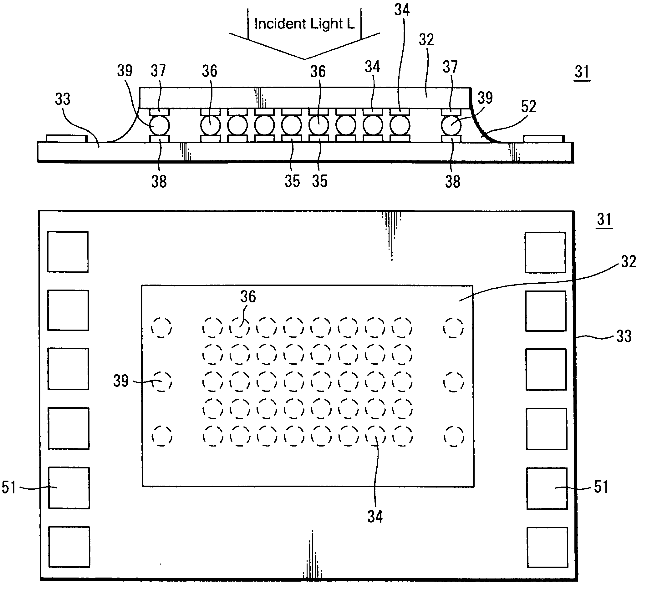
[0082]FIGS. 3A and 3B show a fundamental structure of a semiconductor module according to an embodiment of the present invention. More specifically, FIG. 3A is a side view showing a semiconductor module according to an embodiment of the present invention and FIG. 3B is a plan view thereof.

[0083]A semiconductor module, generally depicted by reference numeral 31 in FIGS. 3A and 3B, includes a MOS type solid-state image pickup device (hereinafter referred to as a “MOS type image sensor chip”) 32 and a signal processing chip (that is, DSP (digital signal processing) chip) 33 which are laminated with each other. As shown in FIGS. 3A and 3B, the signal processing chip 33 is connected to the MOS type image sensor chip 32 and processes an output supplied from the MOS type image sensor chip 32. Further, it is needless to say that the signal processing chip 33 may have a function to control the MOS type ima...


PUM


Abstract

A back-illuminated type MOS (metal-oxide semiconductor) solid-state image pickup device 32 in which micro pads 34, 37 are formed on the wiring layer side and a signal processing chip 33 having micro pads 35, 38 formed on the wiring layer at the positions corresponding to the micro pads 34, 37 of the MOS solid-state image pickup device 32 are connected by micro bumps 36, 39. In a semiconductor module including the MOS type solid-state image pickup device, at the same time an image processing speed can be increased, simultaneity within the picture can be realized and image quality can be improved, a manufacturing process can be facilitated, and a yield can be improved. Also, it becomes possible to decrease a power consumption required when all pixels or a large number of pixels is driven at the same time.

Description

CROSS REFERENCES TO RELATED APPLICATIONS[0001]The present invention contains subject matter related to Japanese Patent Application JP 2004-224208 filed in the Japanese Patent Office on Jul. 30, 2004, the entire contents of which being incorporated herein by reference.BACKGROUND OF THE INVENTION[0002]1. Field of the Invention[0003]The present invention relates to a semiconductor module including a MOS (metal-oxide semiconductor) type solid-state image pickup device, a MOS type solid-state image pickup device, a camera and a method of manufacturing a camera.[0004]2. Description of the Related Art[0005]So far a MOS camera module, for example, is known as a semiconductor module including a MOS type solid-state image pickup device. In order to manufacture a small MOS camera module, there is a promising method of overlaying a MOS type solid-state image pickup device (hereinafter referred to as an “MOS image sensor chip”) and a signal processing chip with each other.[0006]As a MOS camera m...

Claims


Application Information

Patent Timeline
Patent Type & Authority Patents(United States)
IPC IPC(8): H04N3/14H04N5/335H01L25/065H01L25/07H01L25/18H01L27/14H04N5/374
CPCH01L24/17H01L27/14634H01L27/14636H01L27/14643H04N5/335H04N5/37457H01L27/14689H04N5/374H04N5/3745H01L2924/13091H01L2224/16225H01L2224/73204H01L2924/01033H01L2924/01059H01L2924/01082H01L2924/01005H01L2924/01006H01L2924/01047H01L2924/014H01L2924/00H01L2924/12043H01L24/14H01L2224/32225H01L2224/05573H01L2224/05568H01L2924/00014H01L2224/0554H01L27/14612H01L27/1464H01L2224/0615H04N25/00H04N25/79H01L2224/05599H01L2224/0555H01L2224/0556H01L27/14H04N25/76H04N25/77H04N25/778
Inventor MABUCHI, KEIJIURASAKI, SHUNICHI
Owner SONY CORP
Why Eureka
Try Eureka