Semiconductor device and driving method of semiconductor device

a semiconductor and driving method technology, applied in static storage, information storage, digital storage, etc., can solve the problems of high cost per storage capacity, difficult to sufficiently reduce power consumption, short data holding period, etc., to achieve the effect of reducing power consumption, reducing frequency of refresh operation, and reducing power consumption

Active Publication Date: 2013-08-13
SEMICON ENERGY LAB CO LTD
View PDF174 Cites 45 Cited by
  • Summary
  • Abstract
  • Description
  • Claims
  • Application Information

AI Technical Summary

Benefits of technology

[0011]In one embodiment of the disclosed invention, a semiconductor device is formed using a material capable of sufficiently reducing the off-state current of a transistor, such as an oxide semiconductor material that is a widegap semiconductor. The use of a semiconductor material capable of sufficiently reducing the off-state current of a transistor allows data to be held for a long time.
[0021]Since the off-state current of transistors including an oxide semiconductor is extremely small, stored data can be held for an extremely long time owing to such transistors. In other words, refresh operation becomes unnecessary or the frequency of the refresh operation can be extremely lowered, which leads to a sufficient reduction in power consumption. Moreover, stored data can be held for a long period even when power is not supplied (note that a potential is preferably fixed).
[0022]Further, in the semiconductor device according to the disclosed invention, high voltage is not needed for writing data and there is no problem of deterioration of elements. For example, unlike a conventional nonvolatile memory, it is not necessary to inject and extract electrons into and from a floating gate, and thus a problem such as deterioration of a gate insulating layer does not arise at all. That is, the semiconductor device according to the disclosed invention does not have a limitation on the number of times data can be rewritten, which is a problem of a conventional nonvolatile memory, and the reliability thereof is drastically improved. Furthermore, since data is written by turning on or off the transistors, high-speed operation can be easily realized. Additionally, there is an advantage in that operation for erasing data is not needed.
[0023]Since a transistor including a material other than an oxide semiconductor can operate at sufficiently high speed, when this is combined with a transistor including an oxide semiconductor, a semiconductor device can perform operation (e.g., data reading) at sufficiently high speed. Further, a transistor including a material other than an oxide semiconductor can favorably realize a variety of circuits (e.g., a logic circuit or a driver circuit) which needs to operate at high speed.

Problems solved by technology

Moreover, a transistor included in a memory element has leakage current (off-state current) between a source and a drain in an off state or the like and electric charge flows into or out of the transistor even if the transistor is not selected, which makes a data holding period short.
For that reason, write operation (refresh operation) is necessary at predetermined intervals, and it is difficult to sufficiently reduce power consumption.
Furthermore, since stored data is lost when power supply stops, another memory device utilizing a magnetic material or an optical material is needed in order to hold the data for a long time.
However, cost per storage capacity is high because a circuit such as a flip-flop is used.
Moreover, as in a DRAM, stored data in an SRAM is lost when power supply stops.
However, in a flash memory, there is a problem in that a memory element becomes unable to function after a predetermined number of writing operations because a gate insulating layer included in the memory element deteriorates due to tunneling current generated in writing operations.
Moreover, even when such a method is employed, the fundamental problem of lifetime cannot be resolved.
In other words, a flash memory is not suitable for applications in which data is frequently rewritten.
Further, it takes a relatively long time to inject or remove electric charge, and it is not easy to increase the speed of writing or erasing data.

Method used


Image

  • Semiconductor device and driving method of semiconductor device
  • Semiconductor device and driving method of semiconductor device
  • Semiconductor device and driving method of semiconductor device

Examples


embodiment 1

[0062]Structures of semiconductor devices according to one embodiment of the present invention will be described with reference to FIG. 1, FIGS. 2A and 2B, FIGS. 3A to 3C, FIGS. 4A to 4C, FIG. 5, FIG. 6, FIG. 7, and FIG. 8.

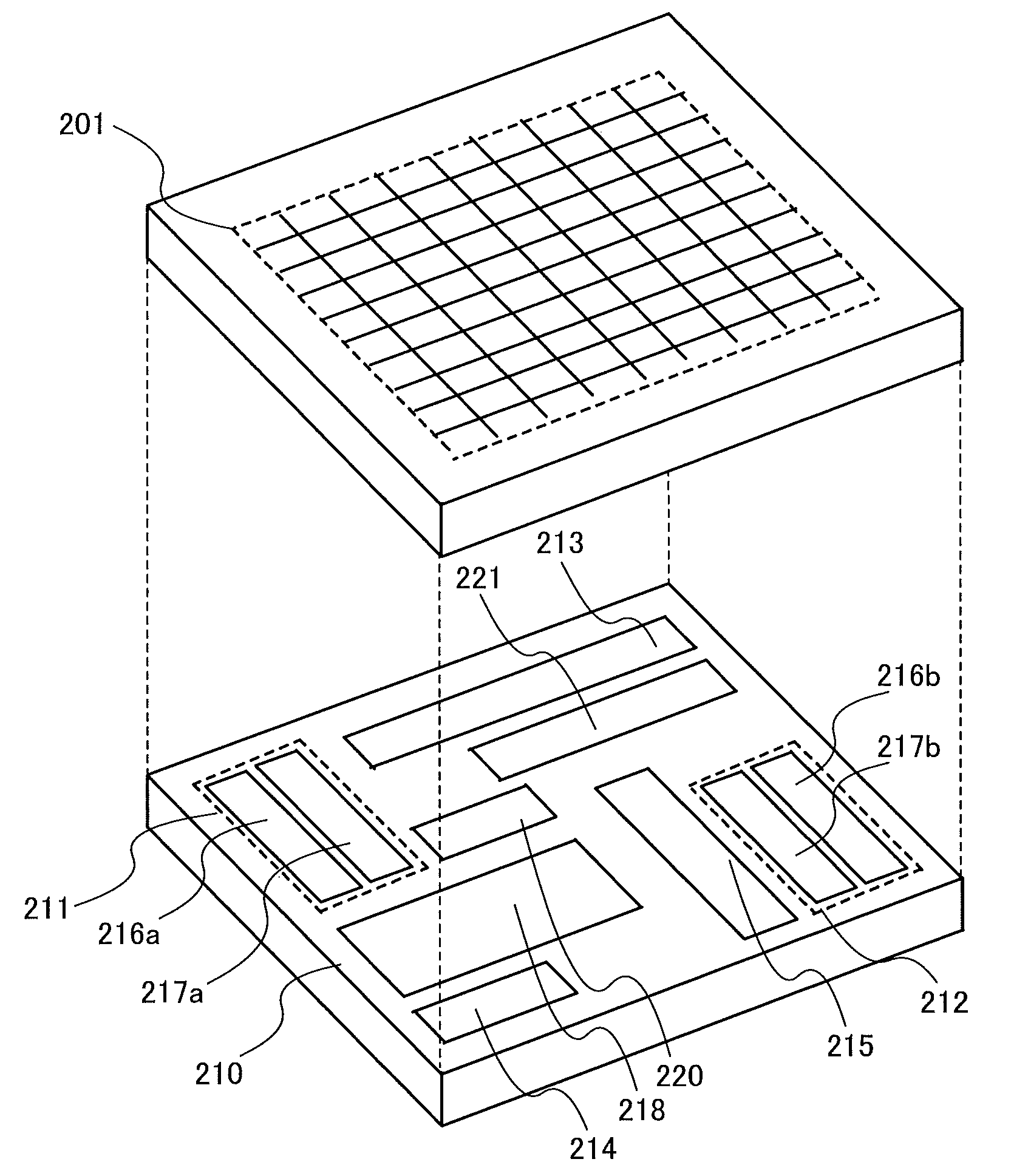
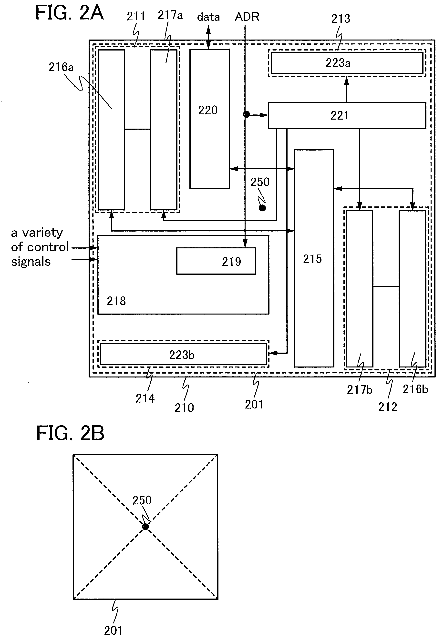
[0063]FIG. 1 is a schematic diagram illustrating an example of a structure of a semiconductor device. The semiconductor device according to one embodiment of the present invention has a stacked-layer structure and includes a memory circuit in an upper portion and a peripheral circuit including a driver circuit, a control circuit, and the like, which needs to operate at high speed for driving the memory circuit, in a lower portion. Note that the driver circuit or the control circuit may be a logic circuit. The peripheral circuit may include an analog circuit, or may include an arithmetic circuit.

[0064]The semiconductor device illustrated in FIG. 1 includes a memory cell array 201 including a plurality of memory cells as a memory circuit in an upper portion and a pe...

embodiment 2

[0130]In this embodiment, a structure and a manufacturing method of a semiconductor device according to one embodiment of the present invention will be described with reference to FIG. 9, FIGS. 10A and 10B, FIGS. 11A and 11B, FIGS. 12A to 12D, FIGS. 13A to 13E, and FIGS. 14A to 14D.

[0131]FIG. 9 is a cross-sectional view of a semiconductor device. In FIG. 9, A1-A2 is a cross section perpendicular to the channel length direction of a transistor. The semiconductor device illustrated in FIG. 9 includes a memory cell array 201 in an upper portion and a peripheral circuit 210 in a lower portion. The memory cell array 201 in the upper portion includes a transistor 162 including an oxide semiconductor, and the peripheral circuit 210 in the lower portion includes a transistor 160 including a semiconductor material other than an oxide semiconductor. Note that Embodiment 1 can be referred to for details of the memory cell array 201 provided in the upper portion of the semiconductor device and ...

embodiment 3

[0249]One embodiment of an oxide semiconductor layer which can be used for a channel formation region of any of the transistors in the above embodiments will be described with reference to FIGS. 14A to 14D.

[0250]The oxide semiconductor layer of this embodiment has a structure including a first crystalline oxide semiconductor layer and a second crystalline oxide semiconductor layer which is stacked over the first crystalline oxide semiconductor layer and has a larger thickness than the first crystalline oxide semiconductor layer.

[0251]A first oxide semiconductor film with a thickness greater than or equal to 1 nm and less than or equal to 10 nm is formed over an insulating layer 140.

[0252]In this embodiment, an oxide insulating layer with a thickness greater than or equal to 50 nm and less than or equal to 600 nm is formed as the insulating layer 140 by a PCVD method or a sputtering method. For example, a single layer selected from a silicon oxide film, a gallium oxide film, an alumi...


PUM


Abstract

An object is to provide a semiconductor device having a novel structure, which can hold stored data even when not powered and which has an unlimited number of write cycles. A semiconductor device is provided with both a memory circuit including a transistor including an oxide semiconductor (in a broader sense, a transistor whose off-state current is sufficiently small) and a peripheral circuit such as a driver circuit including a transistor including a material other than an oxide semiconductor (in other words, a transistor capable of operating at sufficiently high speed). The peripheral circuit is provided in a lower portion and the memory circuit is provided in an upper portion; thus, the area and size of the semiconductor device can be decreased.

Description

TECHNICAL FIELD[0001]An embodiment of the invention disclosed herein relates to a semiconductor device including a semiconductor element and a driving method of the semiconductor device.BACKGROUND ART[0002]Memory devices including semiconductor elements are broadly classified into two categories: volatile memory devices that lose stored data when not powered, and nonvolatile memory devices that hold stored data even when not powered.[0003]A typical example of volatile memory devices is a dynamic random access memory (DRAM). A DRAM stores data in such a manner that a transistor included in a memory element is selected and electric charge is stored in a capacitor.[0004]When data is read from a DRAM, electric charge in a capacitor is lost according to the above-described principle; thus, another write operation is necessary every time data is read out. Moreover, a transistor included in a memory element has leakage current (off-state current) between a source and a drain in an off stat...

Claims


Application Information

Patent Timeline
Patent Type & Authority Patents(United States)
IPC IPC(8): G11C5/02G11C5/06G11C11/24
CPCG11C5/025
Inventor YAMAZAKI, SHUNPEIKOYAMA, JUNKATO, KIYOSHI
Owner SEMICON ENERGY LAB CO LTD
Why Eureka
Try Eureka