Surface-mountable piezoelectric devices including eutectic-bonded packages

a piezoelectric device and package technology, applied in piezoelectric/electrostrictive/magnetostrictive devices, piezoelectric/electrostriction/magnetostriction machines, semiconductor devices, etc., can solve the problems of molten metal porosity, deficiency of package sealing midway between the loci, and inability to protect the base material in conventional devices. , to achieve the effect of preventing porosity formation and uniform thickness of sold

Inactive Publication Date: 2013-09-10
NIHON DEMPA KOGYO CO LTD
View PDF8 Cites 8 Cited by
  • Summary
  • Abstract
  • Description
  • Claims
  • Application Information

AI Technical Summary

Benefits of technology

[0018]In view of the foregoing, the present invention provides, inter alia, piezoelectric devices in which the frame-shaped metallic films and / or the mounting terminals comprise a layer of chromium (Cr), a nickel-tungsten (NiW) alloy layer formed on the surface of the Cr layer, and a gold layer (Au) formed on the surface of the NiW alloy layer. This combination of layers prevents package-sealing failures and prevents weakening of eutectic joint strength between the base-substrate and the cover of the device.
[0029]The solder used in any of the various embodiments summarized above can comprise a eutectic alloy. When such a solder is melted by application of heat, the NiW alloy of the shielding layer is unlikely to diffuse into the gold surface layer, as applicants have discovered from experimentation. As a result, even if molten eutectic draws Au out of the surface layer, the underlying base material is not and does not become exposed on the surface of the package. Thus, formation of porosities (which expose the base material in conventional devices) is prevented. The solder flows uniformly over the surfaces of the frame-shaped metallic films and / or the mounting electrodes to produce a substantially uniform thickness of the solder as a function of distance.

Problems solved by technology

However, conventional quartz-crystal vibrators configured and produced as summarized above (specifically by melting the eutectic balls to produce eutectic melt that must flow over the frame-shaped metallic films 6a, 6b) have a problem in which the air-tightness by which the base-substrates and corresponding covers are bonded together is often compromised. FIG. 13A depicts a eutectic ball 10A placed on a shallow hole 11 at a locus at which four frame-shaped metallic films 6a come nearly together.
As a result of these phenomena, package sealing midway between the loci tends to be deficient.
Although not shown in the figures, another problem that arises whenever one of these conventional piezoelectric devices is mounted on a printed circuit board by soldering is inter-diffusion of elements between the mounting terminals 7 and the solder, which produces porosities in the molten metal.

Method used


Image

  • Surface-mountable piezoelectric devices including eutectic-bonded packages
  • Surface-mountable piezoelectric devices including eutectic-bonded packages
  • Surface-mountable piezoelectric devices including eutectic-bonded packages

Examples


first embodiment

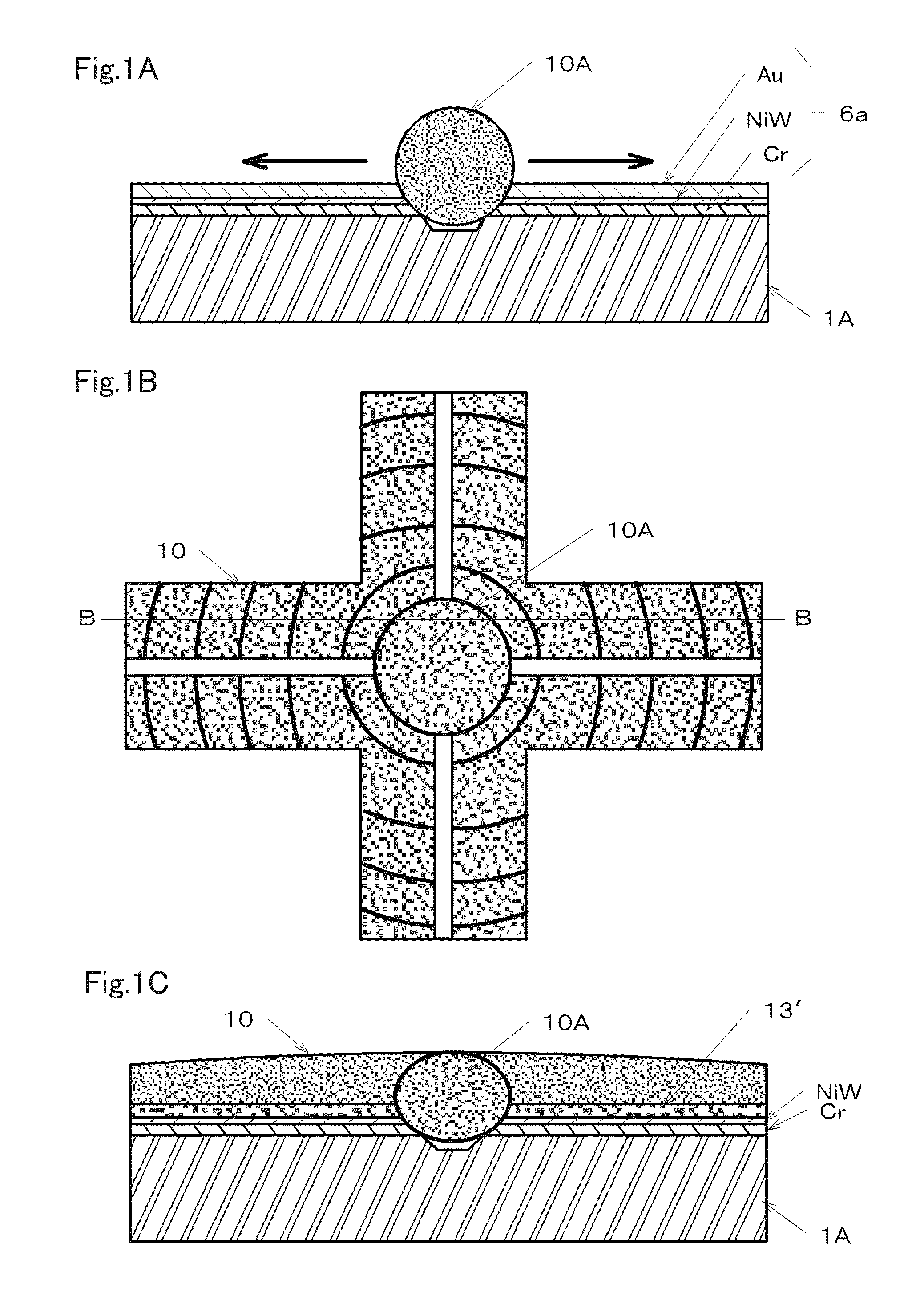
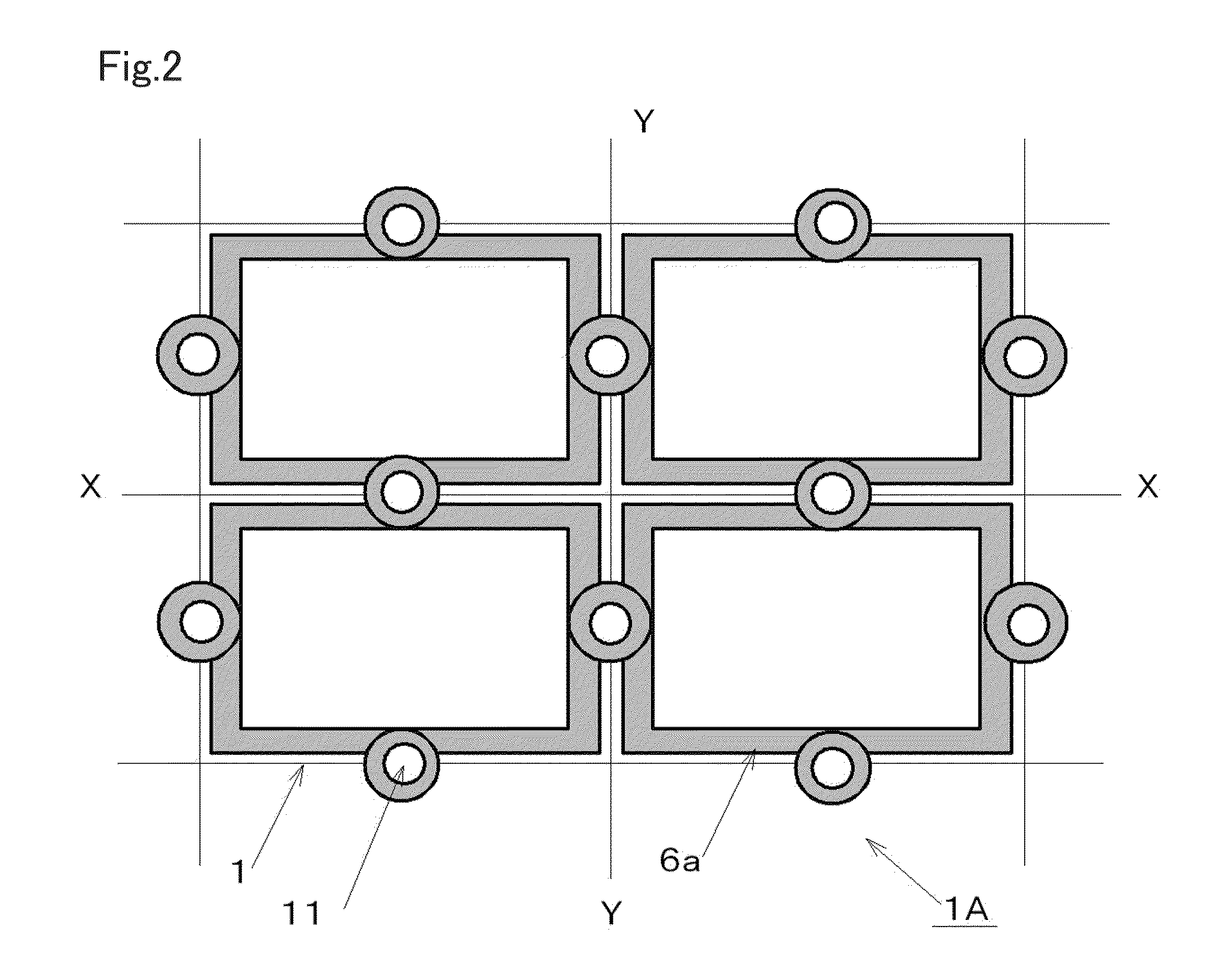
[0044]This embodiment is described below with reference to FIGS. 1A-1C, each depicting a respective view of an “intersection area” in a base-substrate wafer, wherein the intersection area includes the locus at which a respective eutectic ball is placed. In the description of this embodiment, features that are identical to corresponding features in the conventional base-substrate wafer summarized above have the same respective reference numerals and are not detailed further below.

[0045]This embodiment, similar to the conventional quartz-crystal vibrator summarized above and shown in FIGS. 10A-10C, comprises a “recessed” cover 2 (i.e., a cover having an inner main surface defining a concavity). The recessed cover 2 is bonded to a planar base-substrate 1 that comprises a quartz-crystal vibrating piece 4 mounted to its inner main surface and at least one mounting terminal 7 on its lower (outer) main surface. The recessed cover 2 and base-substrate are bonded and sealed together using a ...

second embodiment

[0054]This embodiment is described below with reference to FIGS. 4A-4B and 5A-5B. in this embodiment, components that are similar to corresponding components in the first embodiment have the same respective reference numerals and are not described further below.

[0055]A quartz-crystal vibrator according to this embodiment comprises a framed quartz-crystal vibrating piece 14, a base-substrate 15, and a cover 16. The framed quartz-crystal vibrating piece 14 is a plate-like member formed of, for example, AT-cut crystal material. The periphery of the quartz-crystal vibrating piece 14a comprises a frame portion 14b that surrounds the actual vibrating portion, wherein the vibrating portion is coupled to the frame portion 14b by a connecting bar 14c located at one end of the quartz-crystal piece 14a. As described above, the quartz-crystal piece 14a includes respective excitation electrodes 4a on both main surfaces thereof. Extraction electrodes 4b connect, via the connecting bar 14c, respec...

third embodiment

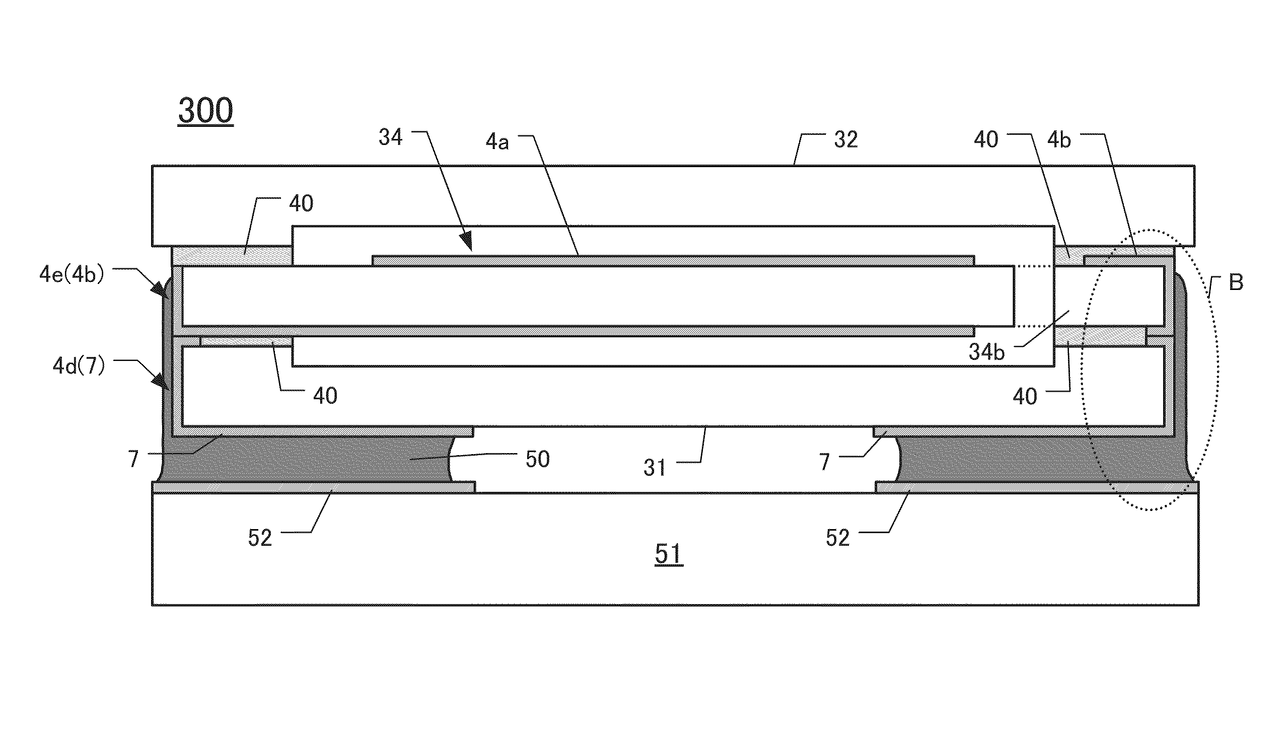
[0063]The quartz-crystal vibrator 300 of this embodiment is mounted on a printed circuit board via the external mounting terminals 7 by soldering (performed with solder paste). The solder material is lead-free and comprises a tin-silver alloy or tin-zinc alloy. These solder pastes have melting points of approximately 220° C. and 190° C., respectively. When either of these alloys flows onto mounting terminals of conventional devices, the solder tends to draw gold from the surfaces of the mounting terminals, which tends to form porosities in the mounting terminals, similar to the porosities shown in FIG. 13, depending on circumstances. These porosities weaken the strength of the bonds between the base- substrate 31 and the mounting terminals 7. To avoid this problem, as described in the first and second embodiments, the mounting terminals 7 of this embodiment are configured with a foundation layer of Cr, a surface layer of Au, and a shielding layer of NiW. The shielding layer is inter...


PUM


Abstract

Piezoelectric devices are disclosed that are mountable on the surface of a printed circuit board or the like. An exemplary device comprises a piezoelectric vibrating piece enclosed and sealed within a package including at least a cover and a base-substrate formed of glass or piezoelectric material. The package includes frame-shaped metallic films formed in peripheral regions of inner main surfaces of the cover and / or the base substrate. The frame-shaped metallic films are used for sealing the package using a eutectic material (e.g., solder). At least one mounting terminal is provided on the outer (bottom) main surface of the base-substrate. At least one of the frame-shaped metallic films and mounting terminals includes a chromium foundation layer formed on the surface of the glass or piezoelectric material, a middle layer of NiW alloy formed on the surface of the chromium layer, and a gold layer formed on the surface of the middle layer.

Description

CROSS-REFERENCE TO RELATED APPLICATIONS[0001]This application claims priority to and the benefit of Japan Patent Application No. 2010-102341, filed on Apr. 27, 2010, and Japan Patent Application No. 2010-236048, filed on Oct. 21, 2010, in the Japan Patent Office, the disclosures of which are incorporated herein by reference in their respective entireties.FIELD[0002]This disclosure pertains to, inter alia, piezoelectric devices in packages sealed with eutectic alloy, wherein the piezoelectric device is mountable on the surface of a printed circuit board or the like. More particularly, the disclosure pertains to electrode structures in such devices that include sealing surfaces (joint faces) and external mounting terminals of a package member, wherein the sealing surfaces and the mounting terminals are bonded, during package assembly, with the eutectic alloy.DESCRIPTION OF THE RELATED ART[0003]The piezoelectric device is known as a frequency-controlling and frequency-selecting element...

Claims


Application Information

Patent Timeline
Patent Type & Authority Patents(United States)
IPC IPC(8): H01L41/053
CPCH03H9/1035H03H9/0519H01L2924/16152
Inventor ICHIKAWA, RYOICHIMIZUSAWA, SHUICHI
Owner NIHON DEMPA KOGYO CO LTD
Why Eureka
Try Eureka