Liquid crystal display device, method for driving the same, and electronic device including the same

a technology of liquid crystal display and liquid crystal, which is applied in the direction of semiconductor devices, instruments, optics, etc., can solve the problems of reducing display quality, power consumption, and difficulty in holding images signals in pixels, so as to reduce power consumption in displaying moving images, still images, or the like, and reduce display quality.

Active Publication Date: 2013-09-10
SEMICON ENERGY LAB CO LTD
View PDF144 Cites 40 Cited by
  • Summary
  • Abstract
  • Description
  • Claims
  • Application Information

AI Technical Summary

Benefits of technology

[0006]In each pixel included in a liquid crystal display device, a storage capacitor for holding the potentials of opposite electrodes which holds a liquid crystal material for a certain period is provided in part of the region of the pixel in order to control the alignment of a liquid crystal element. In order to hold the potentials of the opposite electrodes which holds the liquid crystal material, it is necessary to reduce leakage of electric charge from the opposite electrodes which holds the liquid crystal material. It is important to reduce the off-state current of a thin film transistor connected to a pixel electrode provided in each pixel.
[0009]In view of the foregoing problems, it is an object of one embodiment of the present invention to reduce the off-state current of a thin film transistor and the power consumption of a liquid crystal display device capable of displaying moving images and still images.
[0017]According to one embodiment of the present invention, the off-state current of a thin film transistor including an oxide semiconductor can be reduced, and power consumed in displaying moving images, still images, or the like can be reduced without the decrease in display quality.

Problems solved by technology

Accordingly, even when the image signals in the series of periods are the same, power consumption increases due to rewrite operation of image signals plural times. In this case, even if power consumption is to be reduced by the decrease in the frequency of rewrites of image signals, it is difficult to hold the images signals in pixels due to the increase in off-state current or the like.
Thus, there is concern that display quality will decrease.

Method used


Image

  • Liquid crystal display device, method for driving the same, and electronic device including the same
  • Liquid crystal display device, method for driving the same, and electronic device including the same
  • Liquid crystal display device, method for driving the same, and electronic device including the same

Examples


embodiment 1

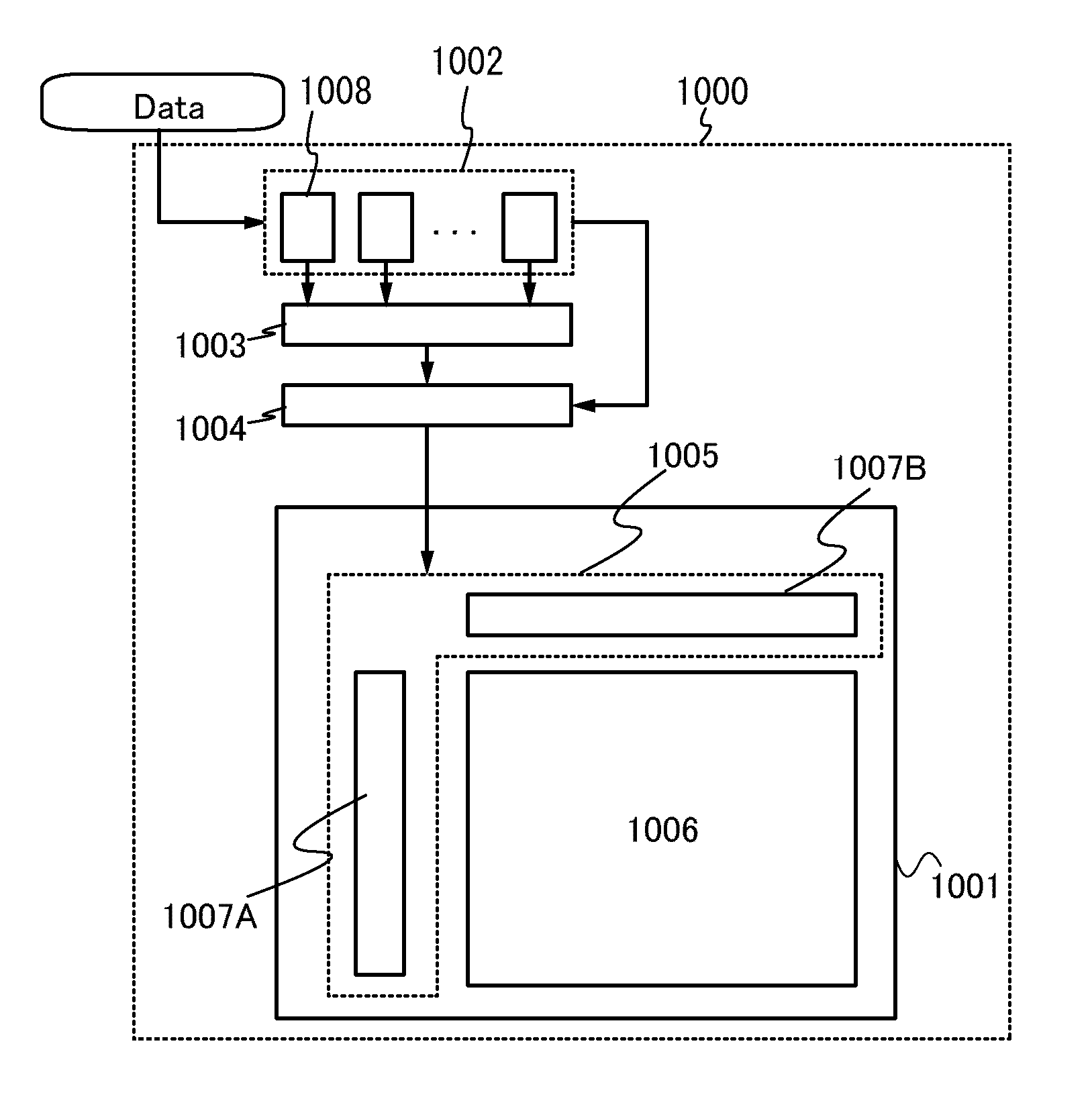
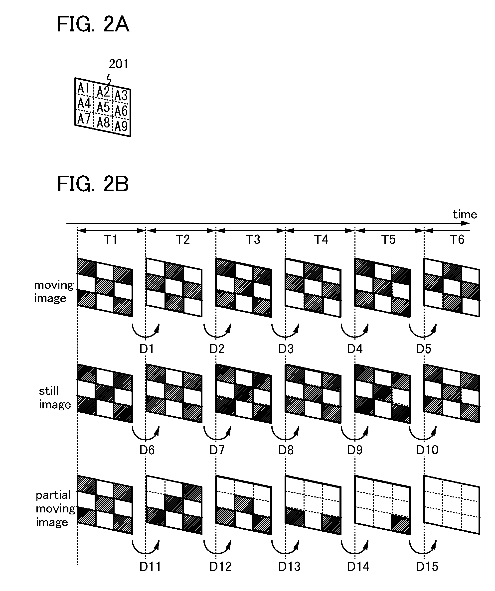
[0041]In this embodiment, a block diagram of a liquid crystal display device and a procedure for determining a moving image, a still image, and a partial moving image are described. First, FIG. 1 illustrates the block diagram of the liquid crystal display device.

[0042]A liquid crystal display device 1000 illustrated in FIG. 1 includes a display panel 1001, a memory circuit 1002, a comparison circuit 1003, and a display control circuit 1004. An image signal Data which is supplied to each pixel is input from the outside.

[0043]The display panel 1001 includes, for example, a driver circuit portion 1005 and a pixel portion 1006.

[0044]The driver circuit portion 1005 includes a gate line driver circuit 1007A and a signal line driver circuit 1007B. The gate line driver circuit 1007A and the signal line driver circuit 1007B are driver circuits for selectively driving a plurality of pixels included in the pixel portion 1006. Specifically, the driver circuit portion 1005 includes a signal line...

embodiment 2

[0130]In this embodiment, in addition to the structure described in the above embodiment, a structure with which voltage can be held for a longer time when a still image is displayed is described. In this embodiment, a schematic diagram, a circuit diagram, and the like of a liquid crystal display device which can be described in addition to the structure in the above embodiment are illustrated, and advantageous effects of the structure in this embodiment are described.

[0131]A liquid crystal display device illustrated in FIG. 6A includes a first substrate 101 and a second substrate 102. The first substrate 101 includes a pixel portion 103, a gate line driver circuit 104, a signal line driver circuit 105, a terminal portion 106, and a switching transistor 107. The second substrate 102 includes a common connection portion 108 (also referred to as a common contact) and a counter electrode 109.

[0132]It is necessary that the first substrate 101 and the second substrate 102 have light-tran...

embodiment 3

[0155]In this embodiment, structures which are different from the structures of the driver circuits and the pixel portion in Embodiment 1 are described with reference to drawings.

[0156]As in FIG. 3A, FIG. 16 illustrates the display control circuit 1004, the pixel portion 1006, the gate line driver circuit 1007A, and the signal line driver circuit 1007B. The pixel portion 1006 includes the plurality of pixels 300. The gate line 301 which extends from the gate line driver circuit 1007 and the signal line 302 which extends from the signal line driver circuit 1007B are connected to each of the pixels 300.

[0157]In addition, the pixel 300 in FIG. 16 includes a thin film transistor 1601 and a liquid crystal element 1602. Note that when a semiconductor layer of the thin film transistor 1601 includes an oxide semiconductor as in Embodiment 1, off-state current can be significantly reduced and the frequency of supplies of image signals when a still image is displayed can be reduced.

[0158]FIG....


PUM

PropertyMeasurementUnit
threshold voltageaaaaaaaaaa
work functionaaaaaaaaaa
band gapaaaaaaaaaa

Abstract

The liquid crystal display device includes a pixel portion including a plurality of pixels to which image signals are supplied; a driver circuit including a signal line driver circuit which selectively controls a signal line and a gate line driver circuit which selectively controls a gate line; a memory circuit which stores the image signals; a comparison circuit which compares the image signals stored in the memory circuit in the pixels and detects a difference; and a display control circuit which controls the driver circuit and reads the image signal in accordance with the difference. The display control circuit supplies the image signal only to the pixel where the difference is detected. The pixel includes a thin film transistor including a semiconductor layer including an oxide semiconductor.

Description

TECHNICAL FIELD[0001]The present invention relates to liquid crystal display devices. Further, the present invention relates to a method for driving liquid crystal display devices. Furthermore, the present invention relates to electronic devices including the liquid crystal display devices.BACKGROUND ART[0002]A thin film transistor formed over a flat plate such as a glass substrate is formed using amorphous silicon or polycrystalline silicon, as typically seen in a liquid crystal display device. Although a thin film transistor including amorphous silicon has low field effect mobility, it can be formed over a larger glass substrate. In contrast, although a thin film transistor including polycrystalline silicon has high field effect mobility, it needs a crystallization process such as laser annealing and the threshold voltage greatly varies, so that such a transistor is not always suitable for a larger glass substrate.[0003]In contrast, attention has been drawn to a technique by which...

Claims


Application Information

Patent Timeline
Patent Type & Authority Patents(United States)
IPC IPC(8): G02F1/136
CPCG02F1/1368G09G3/3659H01L27/1225G09G5/005G02F2202/10G09G2320/103G09G2360/10G09G3/3677
Inventor KOYAMA, JUNYAMAZAKI, SHUNPEI
Owner SEMICON ENERGY LAB CO LTD
Why Eureka
Try Eureka