Method for thermal simulation

a thermal simulation and method technology, applied in the field of thermal analysis and thermal optimization, can solve the problems of heat generation, cost-effective design of ics and systems, dissipation power, etc., and achieve the effects of reasonable computational cost, efficient electro-thermal simulation, and realistic reliability assessmen

Inactive Publication Date: 2013-09-17
CLARKSON UNIVERSITY
View PDF20 Cites 38 Cited by
  • Summary
  • Abstract
  • Description
  • Claims
  • Application Information

AI Technical Summary

Benefits of technology

[0017]In the methods of this invention, thermal simulations of circuits or chips are performed in the hierarchical function space rather than physical space. It is not necessary to use lumped thermal elements such as thermal resistors and capacitors. Our reduced-order model does not require any assumption about dimensions, physical geometry, temperature profiles or heat flow paths in a chip, as usually needed in an efficient approach. This approach not only substantially reduces the computational time but also allows the thermal model to work accurately and efficiently in arbitrarily complex geometries in the domain structures to be simulated.
[0019]The methods also include an approach to efficient electro-thermal simulation in the function space using a circuit simulator (e.g., SPICE), together with appropriate electric models of the components in the structure. In semiconductor technology, for example, these models may include, but not limited to, BSIM models for bulk CMOS and BSIMSOI models for SOI CMOS. Implementing this approach in a circuit simulator will allow chip designers to perform electro-thermal simulations for large functional circuit blocks or chips, at a reasonable computational cost. This will allow them to obtain runtime device junction temperatures and average channel temperatures as well as temperature distributions in interconnects, in order to account for temperature effects on electronic characteristics at different stages of the design flow. For stacked cell structure of a battery pack, the methods can be coupled with the electrochemical models of the battery cells to perform electrochemical-thermal simulation accounting for temperature effects on the electrochemical reaction in each individual cell.
[0020]The efficiency and capability of the methods of the invention will allow designers of ICs and systems to achieve more aggressive but reliable chip design, more realistic reliability assessment, and more effective power / thermal management for thermally aware and cost-effective design. The invention can be applied to any block-based structure. For chip technologies, this may include, but not limited to, bipolar, CMOS, BiCMOS, SOI, MMIC, 3D stacking integration, photonic IC, MEMS, and emerging semiconductor technologies. For other technologies using block-based structures, it may include, but not limited to, photovoltaic panels and battery packs, etc. The methods can be implemented in any CAD or EDA tools for simulations, design, optimization and analysis of devices or systems, where temperature strongly affects their safety, performance and / or reliability. The methods can also be implemented in a standalone single-block structure, such as a chip, a circuit block, a device structure, a battery cell or a battery pack, etc.

Problems solved by technology

The large number of devices and long interconnect lines between devices, cells, and circuit blocks inevitably induce heating problems.
This has become one of the major obstacles to accomplishing cost-effective design of ICs and systems in the semiconductor industry, including not only the conventional digital, analog, RF, and mixed signal CMOS (complementary metal-oxide-semiconductor) technologies but also many other semiconductor technologies, such as BiCMOS (bipolar CMOS), SOI (Silicon-On-Insulator), Bipolar, MMIC (Monolithic Microwave and Millimeter wave IC), and photonic ICs, etc.
The devices, as well as the metal wires and vias, dissipate power and therefore induce thermal heating.
Other semiconductor IC technologies may have different device and / or layout structures; however, thermal gradients and heat exchange between devices and interconnects are inevitable and become more serious as the numbers of devices and interconnects in a chip increase.
It should be mentioned that the miniaturization of devices into nano-scale dimensions also enhances two major problems in semiconductor industry: pronounced short channel effects in the traditional bulk CMOS technology and long interconnect lines in the conventional planar IC structure.
The former gives rise to large leakage power and the channel punch-through characteristics in CMOS devices, and the latter induces long interconnect delays and high power consumption along the long interconnects.
The SOI-based technology however considerably increases self-heating effects because the oxide placed under the device channels to suppress the short-channel effects exacerbates the chip heating problem.
These technologies place the conventional planar circuit blocks or dies vertically to reduce the interconnect lengths and delays but worsens the chip heating problem due to the increase in power density and the difficulty to dissipate heat to the ambient.
These approaches are however computationally time consuming and difficult to use to achieve cost-effective design.
These approximations may not provide accurate heat flow or heat exchange between devices and / or interconnects in complex multi-dimensional IC geometry.
In addition, they are not able to capture high temperature gradients or hot spots in chips.
The internal temperature distributions in stacked battery cells significantly affect performance and reliability of the battery pack.
The non-uniform temperature distribution in the battery pack will thus lead to unbalanced cell impedances and power flow, lower performance and shorter life expectancy.
For some batteries, high cell temperature may also induce thermal runaway and cause safety problems.
Consequently, thermal management in the battery and automotive industries has become one of the major issues for optimizing battery operation, performance, safety and life expectancy.
The detailed temperature profiles in the battery packs are currently derived from numerical thermal simulation, which is very time consuming especially in the dynamic cases.
To account for temperature influences on the electrochemical model of each battery cell, it needs to couple the numerical thermal simulation with the electrochemical model, which substantially increases the simulation time and is prohibitive for realistic applications.
As a result, constant cell temperature is usually assumed to simplify the simulation, which however does not reflect the realistic heat generation, local temperature effects on element parameters of the battery cell electrochemical model, and the heat flow across cells.

Method used


Image

  • Method for thermal simulation
  • Method for thermal simulation
  • Method for thermal simulation

Examples


Embodiment Construction

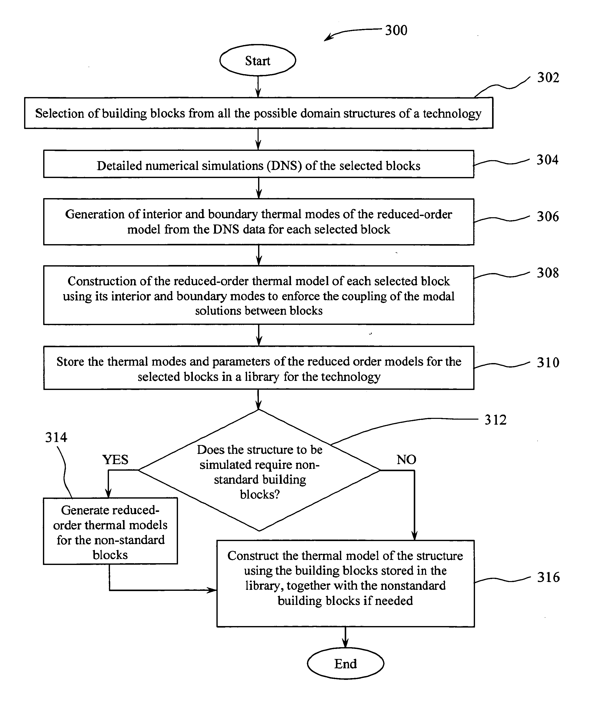
[0042]Embodiments of the present invention provide two efficient and accurate methods for 3D steady-state and transient thermal simulation in a block-based structure, including but not limited to semiconductor chips and packages, photovoltaic modules and panels, and battery packs, etc. The methods are able to obtain the temperature profile in a structure as detailed as a full-scale numerical simulation at a small fraction of the computational cost that is currently possible. In this description, the procedure, theory and concept of the methods of the invention are presented based on semiconductor chips. These can also be applied to other block-based structures.

[0043]The methods can evaluate 3D thermal profiles efficiently at different levels of resolution, as fine as the device junction or average device temperature or as coarse as the average temperature of a standard cell, a large circuit block, or even a die. In addition, the methods can be applied to efficient 3D thermal and ele...


PUM


Abstract

The invention of novel methods is described for efficient and accurate thermal simulation of a structure that can be primarily constructed using building blocks. These structures may include, but not limited to, semiconductor chips, photovoltaic / solar panels, battery packs, etc. The methods are formulated in hierarchical function spaces, rather than the physical space and provide three-dimensional (3D) steady-state and transient temperature profiles of the structure, which are as detailed as full-scale numerical simulation, using substantially less computational degrees-of-freedom (DOF). The number of DOF required is comparable to that of lumped thermal models, yet no ad-hoc modeling assumptions related to geometry, dimensions, temperature profiles, or heat flow paths are required. The methods can be applied to evaluate temperature profiles at different levels of granularity. The methods can also be implemented in various computer-aided-design (CAD) or electronic-design-automation (EDA) tools for different technologies to perform electro-thermal simulations.

Description

CROSS REFERENCE[0001]This application is related to Provisional Patent Application 61 / 129,910 filed on Jul. 29, 2008 entitled Method for Thermal Simulation of Semiconductor Chips and Provisional Patent Application 61 / 199,233 on Nov. 14, 2008 entitled, entitled Method for Thermal Simulation of Structures, both hereby incorporated herein by reference.FIELD OF THE INVENTION[0002]This invention relates in general to thermal analysis and thermal optimization in a domain structure which can be primarily constructed using building blocks, to achieve optimal design of the structure in terms of the performance, reliability, safety, and power and thermal management. More particularly, the invention relates to thermal simulation of the block-based structures including, but not limited to, semiconductor chips and packages, photonic chips and packages, photovoltaic modules and panels, and battery cells and packs, etc.BACKGROUND OF THE INVENTION[0003]The methods of the invention can be applied to...

Claims


Application Information

Patent Timeline
Patent Type & Authority Patents(United States)
IPC IPC(8): G06F17/50
CPCG06F17/5036G06F2217/80G06F30/367G06F2119/08
Inventor CHENG, MING-CHENGHELENBROOK, BRIAN T.
Owner CLARKSON UNIVERSITY
Why Eureka
Try Eureka