

Dicing die bonding film and dicing method
a die bonding film and die bonding technology, applied in the direction of adhesive types, transportation and packaging, layered products, etc., can solve the problems of contaminating patterns, defective semiconductor chips, thin thickness of wafers, etc., to improve workability and reliability in any semiconductor packaging process, reduce the incidence of burrs in the dicing process, and maximize the adhesive property
- Summary
- Abstract
- Description
- Claims
- Application Information
AI Technical Summary
Benefits of technology
Problems solved by technology
Method used
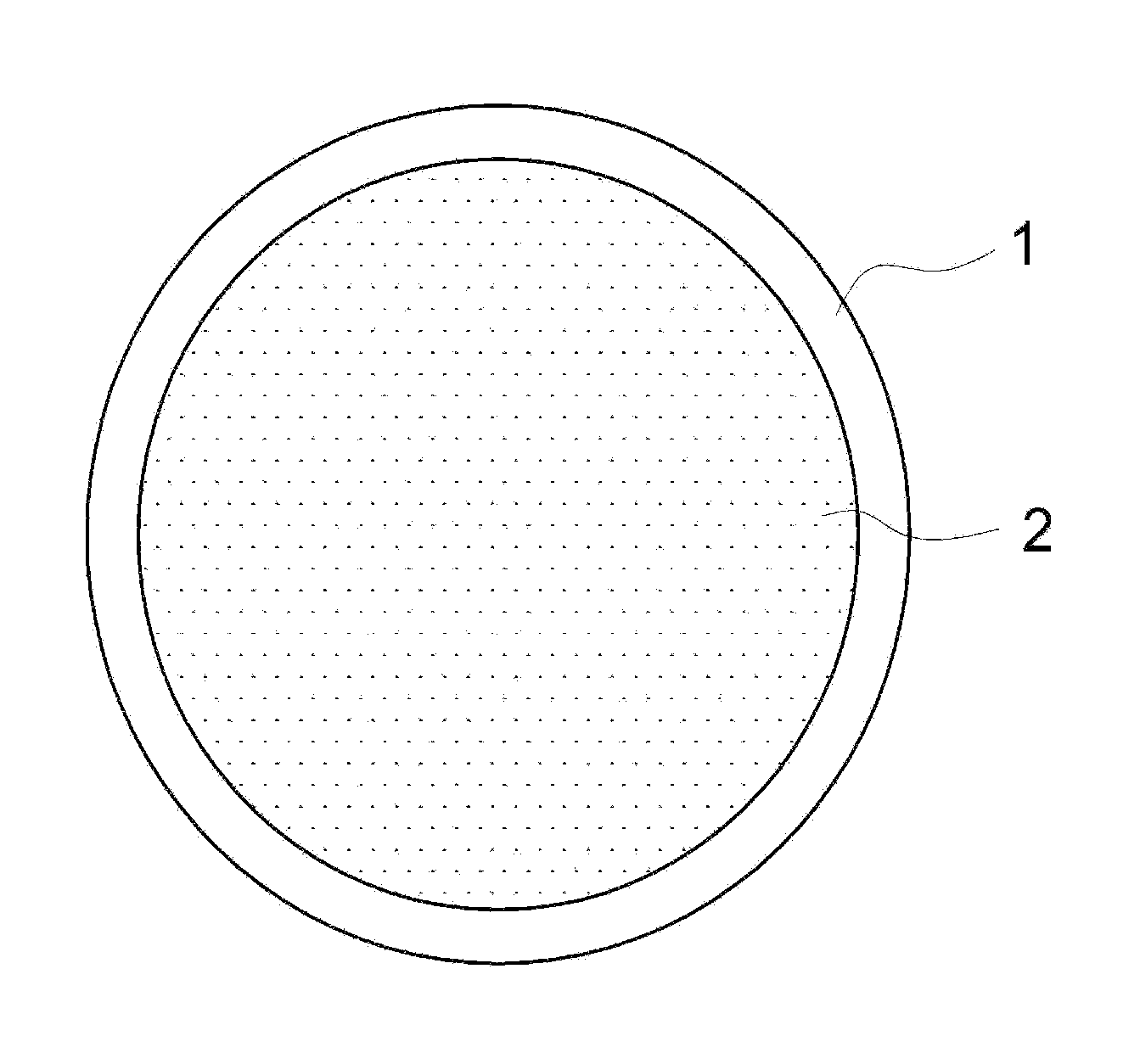
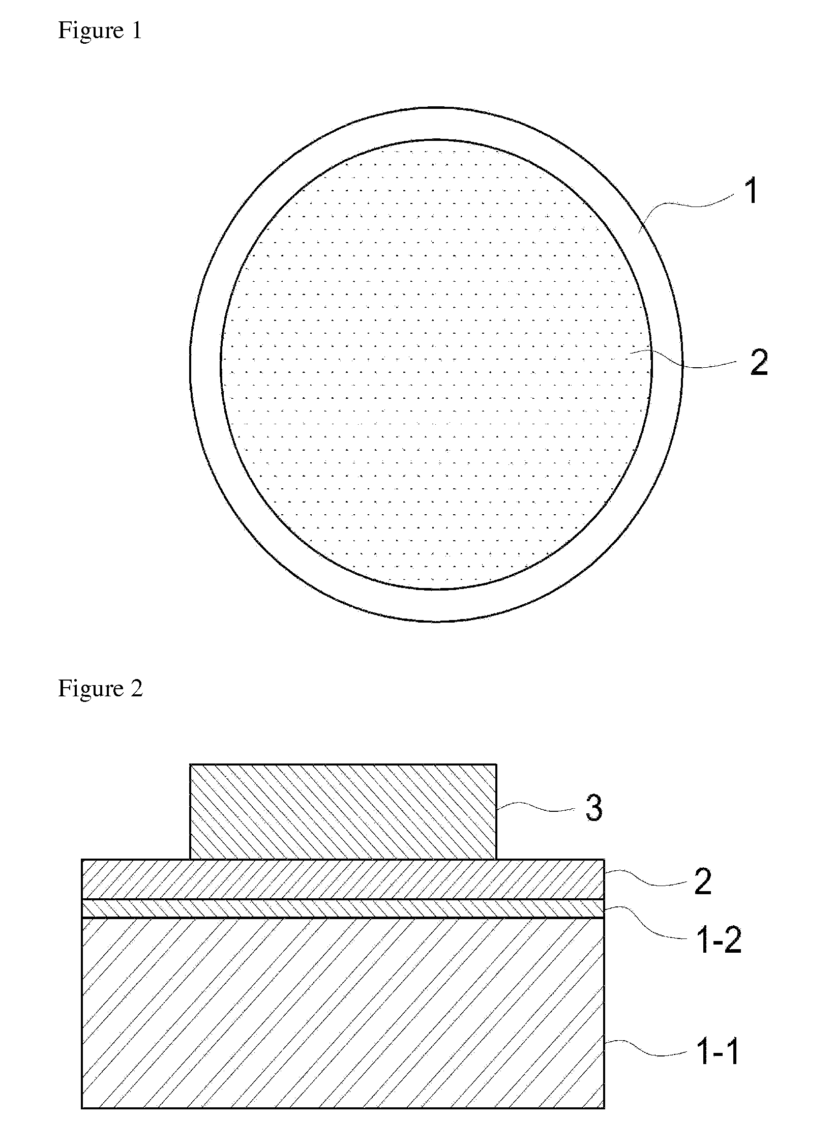
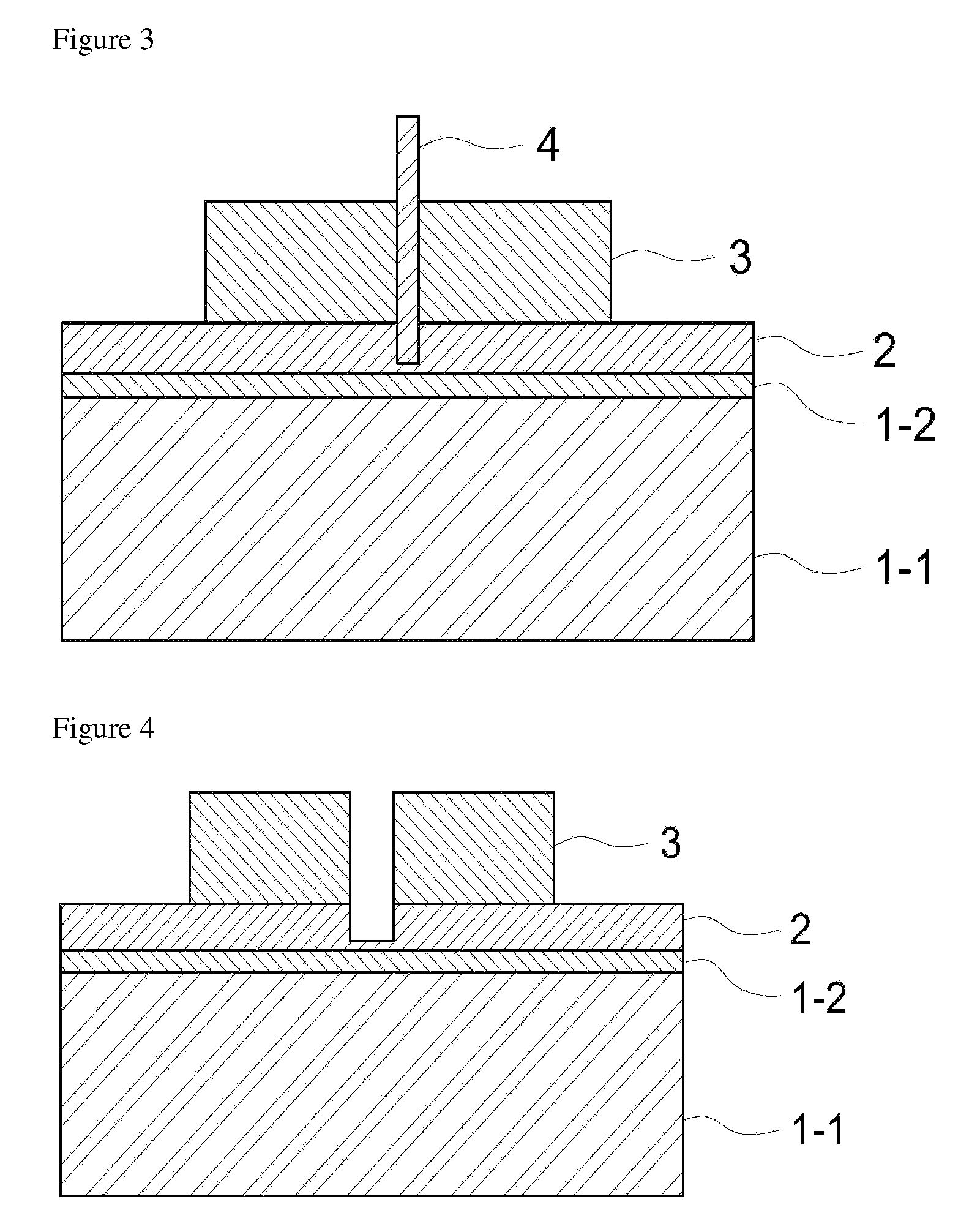
Image

Examples
example 1
[0078]A composition containing 66 parts by weight of an aromatic-based epoxy resin (novolac type epoxy resin, softening point 80° C.), 60 parts by weight of a phenol resin (phenol novolac resin, softening point 90° C.), 200 parts by weight of an acrylic copolymer containing epoxy group (SA-55, manufactured by LG Chem, Ltd., Tg=9° C., weight average molecular weight 500,000), 0.3 parts by weight of a hardening accelerator (2-phenyl-4-methyl imidazole (2P4MZ) and 15 parts by weight of silica (melted silica, average particle diameter 75 nm), was stirred and mixed in methyl ethyl ketone to prepare a varnish.
[0079]The prepared varnish was applied on a base film having a thickness of 38 μm (Release Polyester Film, RS-21G, manufactured by SKC), and dried at 110° C. for 3 minutes to prepare a film having a film thickness of 20 μm. The prepared film was cut in a size of 50 mm×10 mm (length×width), such that the longitudinal direction is the coating direction in preparing, to prepare a specim...
example 2
[0080]A dicing die bonding film was prepared by the same method as Example 1 except that an acrylic resin was used in an amount of 100 parts by weight. Here, the die bonding film had a tensile modulus of 900 MPa.
example 3
[0081]A dicing die bonding film was prepared by the same method as Example 1 except that an acrylic resin was used in an amount of 400 parts by weight. Here, the die bonding film had a tensile modulus of 200 MPa.
PUM
| Property | Measurement | Unit |
|---|---|---|
| length×width | aaaaa | aaaaa |
| size | aaaaa | aaaaa |
| speed | aaaaa | aaaaa |
Abstract
Description
Claims
Application Information