Formation of a graphene layer on a large substrate

a graphene layer and substrate technology, applied in the direction of basic electric elements, electrical equipment, semiconductor devices, etc., can solve the problems of limited epitaxy formation of graphene on a hexagonal surface of silicon carbide crystals, inability to provide 200 mm substrates or 300 mm substrates containing graphene layers, and inability to perform epitaxy on substrates having a diameter of 6 inches or greater, etc., to achieve the effect of low cos

Active Publication Date: 2013-09-24
GLOBALFOUNDRIES US INC
View PDF7 Cites 4 Cited by
  • Summary
  • Abstract
  • Description
  • Claims
  • Application Information

AI Technical Summary

Benefits of technology

[0009]A single crystalline silicon carbide layer can be grown on a single crystalline sapphire substrate. Subsequently, a graphene layer can be formed by conversion of a surface layer of the single crystalline silicon layer by performing an anneal at an elevated temperature in a vacuum environment. Alternately, a graphene layer can be deposited on an exposed surface of the single crystalline silicon carbide layer. A graphene layer can also be formed directly on a surface of a sapphire substrate or directly on a surface of a silicon carbide substrate. The commercial availability of sapphire substrates and semiconductor substrates with a diameter of six inches or more allows formation of a graphene layer on a commercially scalable substrate for low cost manufacturing of devices employing a graphene layer.

Problems solved by technology

Such unavailability of silicon carbide (SiC) substrates currently makes it impossible to provide a 200 mm substrate or a 300 mm substrate containing a graphene layer.
Thus, formation of graphene by epitaxy on a hexagonal surface of a silicon carbide crystal is limited to epitaxial deposition process performed directly on commercially available silicon carbide substrates having a hexagonal symmetry, but cannot be performed on substrates having a diameter of 6 inches or greater.
Growing high quality graphene on SiC grown on Si by subtractive epitaxy is complicated, due to the fact that the Si substrate melts around 1400° C., and high quality graphene is preferably formed at a temperature greater than 1400° C. Furthermore, even if graphene is formed below 1400° C., there will be a quite substantial Si vapor pressure in the vicinity of SiC, due to the presence of the Si substrate, which may suppress the sublimation of Si from SiC needed to form graphene (see for example Tromp and Hannon Phys. Rev. Lett. 102, 106104 (2009)).

Method used


Image

  • Formation of a graphene layer on a large substrate
  • Formation of a graphene layer on a large substrate
  • Formation of a graphene layer on a large substrate

Examples


first embodiment

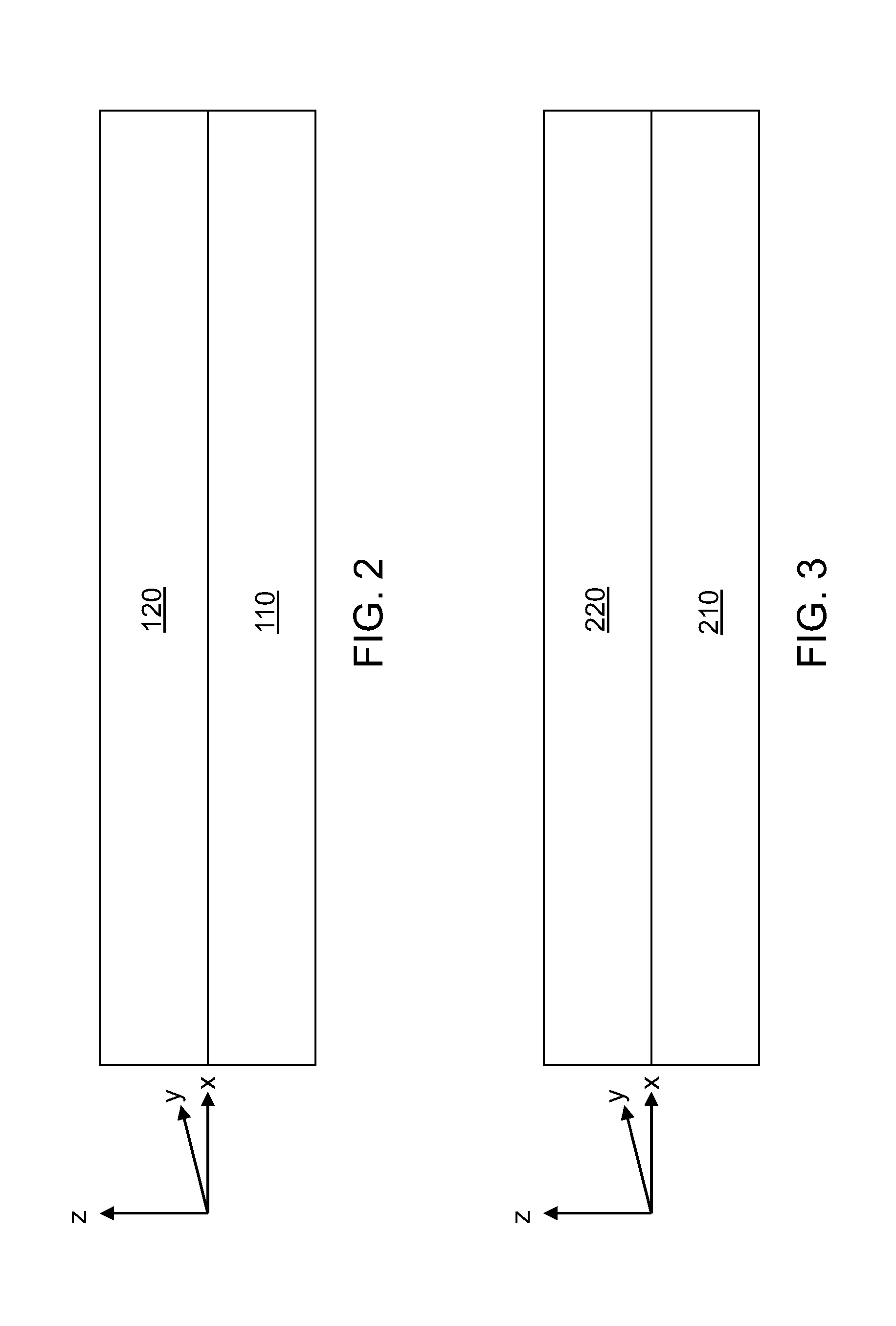
[0053]Referring to FIG. 2, a first exemplary structure including according to the present invention includes a vertical stack of a single crystalline semiconductor-carbon alloy layer 120 and a sapphire substrate 110. The single crystalline semiconductor-carbon alloy layer 120 has a hexagonal crystal structure and a (0001) surface orientation. The single crystalline semiconductor-carbon alloy layer 120 is epitaxially deposited on a (0001) surface of the sapphire substrate 110.

[0054]The sapphire substrate 110 consists essentially of aluminum oxide, i.e., Al2O3, and may include trace amounts of impurities at concentrations that do not affect the crystal structure of the sapphire substrate 110. Typically, the trace amounts of impurities do not exceed 0.02% in atomic concentration. The entirety of the sapphire substrate 110 is single crystalline. Sapphire substrates are currently commercially available at diameters up to 8 inches. The surface orientation of the sapphire substrate 110 is ...

second embodiment

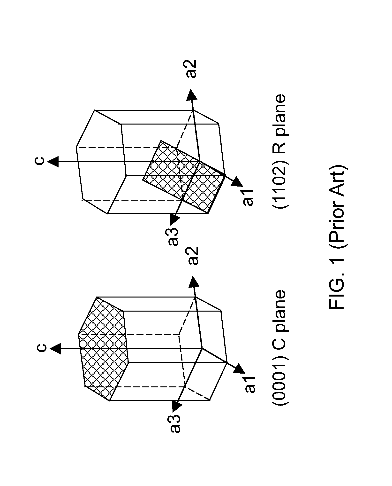
[0061]Referring to FIG. 3, a second exemplary structure including according to the present invention includes a vertical stack of a single crystalline semiconductor-carbon alloy layer 220 and a sapphire substrate 210. The single crystalline semiconductor-carbon alloy layer 220 has a cubic crystal structure of zinc blende type and a (110) surface orientation. The single crystalline semiconductor-carbon alloy layer 220 is epitaxially deposited on a (1102) surface of the sapphire substrate 210.

[0062]The sapphire substrate 210 consists essentially of aluminum oxide as in the first embodiment. The entirety of the sapphire substrate 210 is single crystalline. However, the surface orientation of the sapphire substrate 210 is a (1102) orientation. The plane of the (1102) orientation is also referred to as an R plane.

[0063]The single crystalline semiconductor-carbon alloy layer 220 is a single crystalline layer in which all atoms are epitaxially aligned to all other atoms of the single cryst...

third embodiment

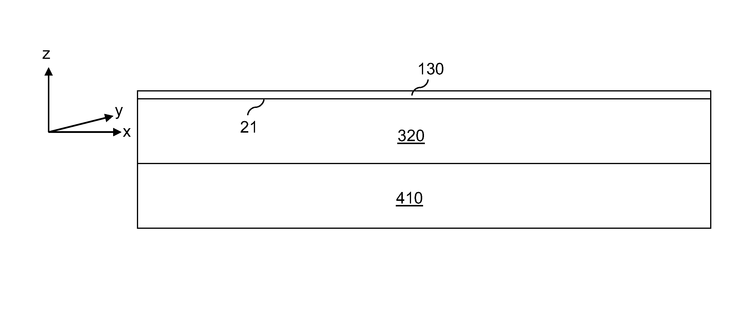
[0086]Referring to FIG. 16, a third exemplary structure according to the present invention includes a stack of a graphene layer 30 formed by graphitization, a single crystalline semiconductor-carbon alloy layer 120, and a sapphire substrate 110 having a (0001) surface orientation. The single crystalline semiconductor-carbon alloy layer 120 has a hexagonal crystal structure, i.e., in alpha phase. The third exemplary structure is derived from the first exemplary structure by graphitizing a surface portion of the single crystalline semiconductor-carbon alloy layer 120. Specifically, the graphene layer 30 is formed directly on the top surface 21 of a remaining portion of the single crystalline semiconductor-carbon alloy layer 120 by conversion of a top layer of the single crystalline semiconductor-carbon alloy layer 120. The conversion can be effected by evaporating semiconductor atoms from the top layer at an elevated temperature, for example, from 800° C. to 2,000° C. The graphene lay...


PUM

PropertyMeasurementUnit
temperatureaaaaaaaaaa
thicknessaaaaaaaaaa
lengthaaaaaaaaaa

Abstract

A single crystalline silicon carbide layer can be grown on a single crystalline sapphire substrate. Subsequently, a graphene layer can be formed by conversion of a surface layer of the single crystalline silicon layer during an anneal at an elevated temperature in an ultrahigh vacuum environment. Alternately, a graphene layer can be deposited on an exposed surface of the single crystalline silicon carbide layer. A graphene layer can also be formed directly on a surface of a sapphire substrate or directly on a surface of a silicon carbide substrate. Still alternately, a graphene layer can be formed on a silicon carbide layer on a semiconductor substrate. The commercial availability of sapphire substrates and semiconductor substrates with a diameter of six inches or more allows formation of a graphene layer on a commercially scalable substrate for low cost manufacturing of devices employing a graphene layer.

Description

STATEMENT REGARDING FEDERALLY SPONSORED RESEARCH OR DEVELOPMENT[0001]This invention was made with government support under Defense Advanced Research Project Agency (DARPA) CERA Contract No. FA8650-08-C-7838 awarded by the U.S. Department of Defense. The government has certain rights in this invention.RELATED APPLICATIONS[0002]The present application is related to co-assigned and co-pending U.S. application Ser. Nos. 12 / 844,029 filed on Jul. 27, 2010 and 12 / 942,498 (being filed on the same date herewith).BACKGROUND[0003]The present invention relates to methods of forming a graphene layer on commercially available large substrates, and structures obtained by the same.[0004]Graphene is a structure consisting of carbon as a two-dimensional sheet. A graphene monolayer has a thickness of about 0.34 nm, i.e., which is approximately the van der Waals atomic diameter of a single carbon atom. As defined by IUPAC, graphene is a one-atom thick, two-dimensional (2D) sheet of C atoms arranged in ...

Claims


Application Information

Patent Timeline
Patent Type & Authority Patents(United States)
IPC IPC(8): H01L29/12
CPCH01L21/02378H01L21/0242H01L21/02447H01L21/02527H01L21/02612H01L21/0262H01L21/02656H01L29/1606H01L29/267
Inventor CHU, JACK O.DIMITRAKOPOULOS, CHRISTOS D.FREITAG, MARCUS O.GRILL, ALFREDMCARDLE, TIMOTHY J.WISNIEFF, ROBERT L.
Owner GLOBALFOUNDRIES US INC
Why Eureka
Try Eureka