

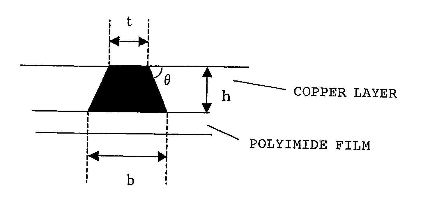
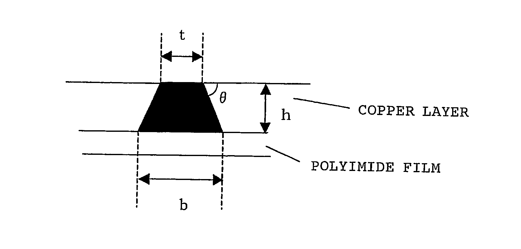
Two-layer flexible substrate
a flexible substrate and two-layer technology, applied in the direction of insulating substrate metal adhesion improvement, synthetic resin layered products, instruments, etc., can solve the problems of wiring defects, and reliance on a complex set of operations, and achieve the effect of improving yield
- Summary
- Abstract
- Description
- Claims
- Application Information
AI Technical Summary
Benefits of technology
Problems solved by technology
Method used
Image

Examples
examples
[0038]The invention is explained next based on examples. The invention, however, is in no way meant to be limited to or by these examples.
examples 1 to 2
, Comparative Examples 1 to 3
[0039]Polyimide films having an underlying metal layer were electroplated under the plating conditions below to prepare copper layers about 8 μm thick. The additives and the amounts thereof are given in Table 1.
[0040]Solution volume: about 800 ml
[0041]Anode: lead electrode
[0042]Cathode: rotating electrode with polyimide film coiled thereon
[0043]Polyimide film having an underlying metal layer: obtained by sputtering NiCr 10 nm thick+Cu 2000 A thick on 37.5 μm-thick Kapton E (DuPont).
[0044]Current duration: 1300 As
[0045]Current density: 5→10→20→30 A / dm2 variation (each current density held for 40 seconds)
[0046]Flow rate: 190 rpm
[0047]Cu: 70 g / L
[0048]H2SO4: 60 g / L
[0049]Cl: 75 ppm
[0050]The surface roughness (Ra) (μm) (arithmetic average roughness) of the obtained copper polyimide two-layer substrates was measured in accordance with JIS B 0601. The average crystal grain size of copper at a position 1 μm from the polyimide film was determined. The number of de...
PUM
| Property | Measurement | Unit |
|---|---|---|
| average crystal grain size | aaaaa | aaaaa |
| average crystal grain size | aaaaa | aaaaa |
| average crystal grain size | aaaaa | aaaaa |
Abstract
Description
Claims
Application Information