Thermopile infrared sensor by monolithic silicon micromachining

a technology of infrared sensor and monolithic silicon, which is applied in the field of thermal infrared sensors, can solve the problems of low residual gas pressure or fill gas cost effective housing structure, insufficient high sensitivity, and slits in the membrane, etc., and achieves high thermal resolution capacity, small chip size, and high degree of filling

Active Publication Date: 2013-11-26
HEIMANN SENSOR GMBH
View PDF25 Cites 17 Cited by
  • Summary
  • Abstract
  • Description
  • Claims
  • Application Information

AI Technical Summary

Benefits of technology

[0028]The object of the invention is to provide a thermopile infrared sensor in monolithic silicon micromachining technology, where said infrared sensor has a high thermal resolution capacity with a small chip size, a high degree of filling and a high response rate and can be operated under gas at normal pressure or reduced pressure and can be mass produced cost effectively with standard CMOS processes without expensive technologies for the housing closure under ultra high vacuum.
[0030]The invention provides a thermopile sensor structure that possesses an especially high signal sensitivity and enables a high degree of filling.
[0033]Furthermore, it can be provided that the thermoelements on long, narrow connecting webs are led around the absorber region. In this case the connecting webs exhibit at least one reversal point. This strategy makes it possible to obtain a meander shape of the connecting webs that, as a result, exhibit a greater length.

Problems solved by technology

In contrast, the cost effective housing structures under low residual gas pressure or with a fill gas do not produce an adequately high sensitivity.
The proposed solution exhibits slits in the membrane that, however, do not permit optimal use of the available area, because such utilization is prevented by the illustrated etching process with the inclined walls.
However, the described arrangement exhibits a plethora of drawbacks.
The process costs rise by a factor of the number of stacked linear arrays that are used; similarly the exact alignment of the individual chips that are stacked one above the other and their connection to each other also means a high technological complexity and financial outlay, and the pixels can be used only to achieve a linear array, because they are not square and are, thus, unsuited for generating a two-dimensional infrared image.
Furthermore, the membrane is structured by rear sided, anisotropic wet etching, a technique that results in a considerable enlargement of the sensor structure owing to the inclined walls of the heat sink.
The aforementioned pairing of materials for the thermopiles (bismuth / antimony) and the absorber material (silver black coating) are barely compatible with the CMOS process.
Another drawback is the high temperature dependence of the sensitivity of the aforementioned material pairing.
The size of the chip as a function of the process leads to relatively high manufacturing costs and again stands in the way of cost effective mass applications.
In both cases the results are produced by a wet etching process that does not permit the occurrence of large distances from the heat sink owing to the inclined walls.
A plurality of parallel arranged thermoelements prevents large temperature differentials between the hot and cold contacts and, thus, a high signal sensitivity cannot be obtained.
200 μm does not enable high sensitivities owing to the heat conductivity of the gas.
However, the small element dimensions on the silicon surface automatically require high vacuum sealed packaging of the sensor chip, a feature that once again is at variance with cost effective mass production.
The possibility of sealing this chip in a cost effective housing with gases of low thermal conductance under normal pressure conditions would drastically reduce the attainable sensitivity.
However, the wide slits prevent optimal utilization of the available area (degree of filling) of the sensor cell.
The inclined substrate walls that run towards the outside do not permit any small sensor cells or short distances between the cells (array structures).
Working on this basis, the prior art solutions propose thermal infrared sensor cells that do not permit a cost effective production of thermal infrared sensor cells exhibiting a high sensitivity and simultaneously a high degree of filling and simple housing technology without a high vacuum sealed housing closure either for reasons relating to the large area chip technology or too little distance between the sensor structure (absorber region) and the support substrate located underneath or for reasons relating to the costly vacuum housing technology.

Method used


Image

  • Thermopile infrared sensor by monolithic silicon micromachining
  • Thermopile infrared sensor by monolithic silicon micromachining
  • Thermopile infrared sensor by monolithic silicon micromachining

Examples


first embodiment

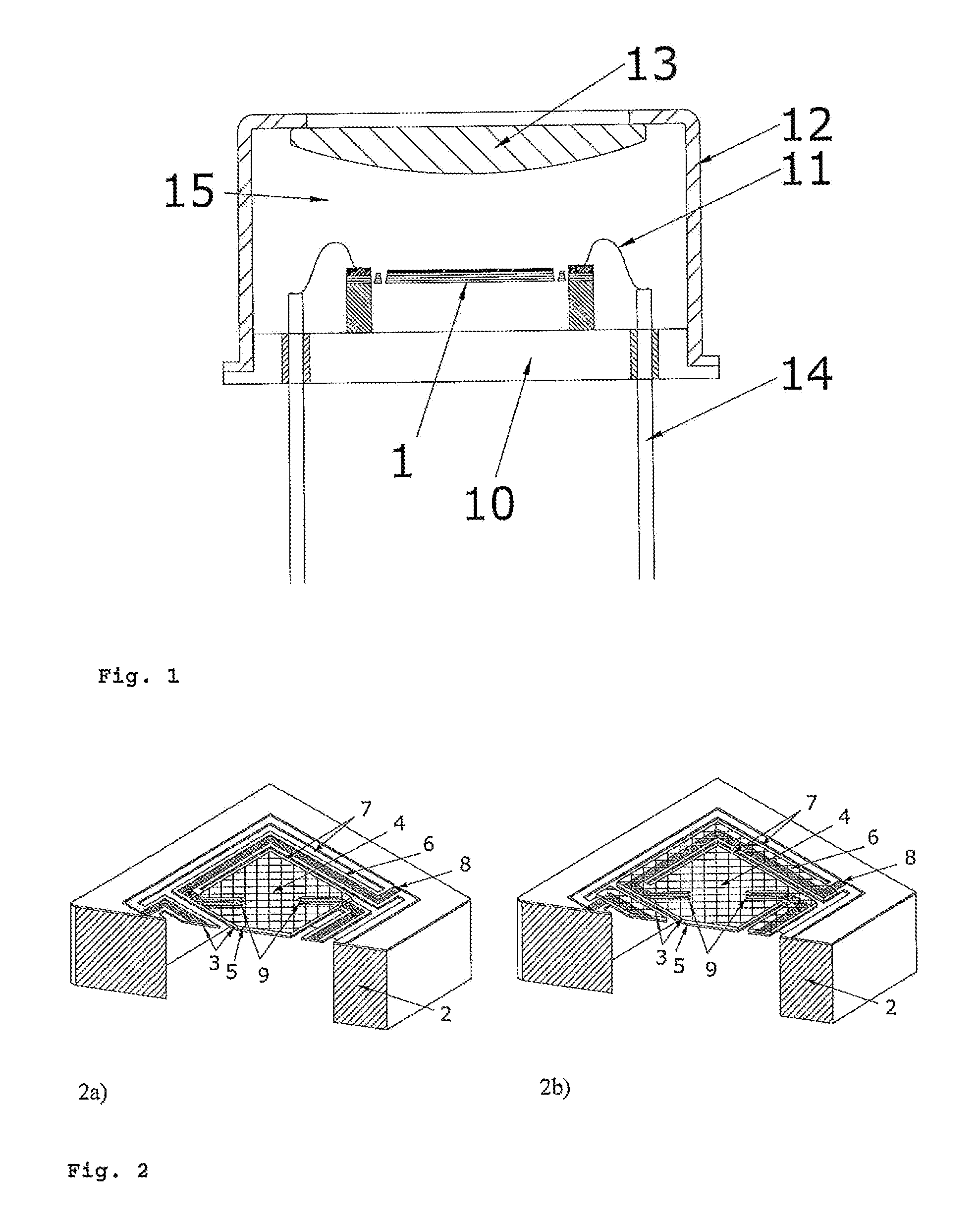
[0095]Two additional embodiments are presented. In the first embodiment the pressure of the surrounding gas is reduced. The best sensitivity is achieved when a vacuum housing structure is used, but intermediate steps are also conceivable. The drawback with the vacuum housing is that the entire housing must be absolutely hermetically gas tight and no change in the gas pressure may occur over several years. This approach necessitates a complex and, thus, costly housing technology.

second embodiment

[0096]In the second embodiment the housing is filled under normal pressure with a gas of lower thermal heat conduction, such as e.g. krypton or xenon. This approach also increases the sensitivity of the sensor, but the requirements with respect to the housing technology are lower.

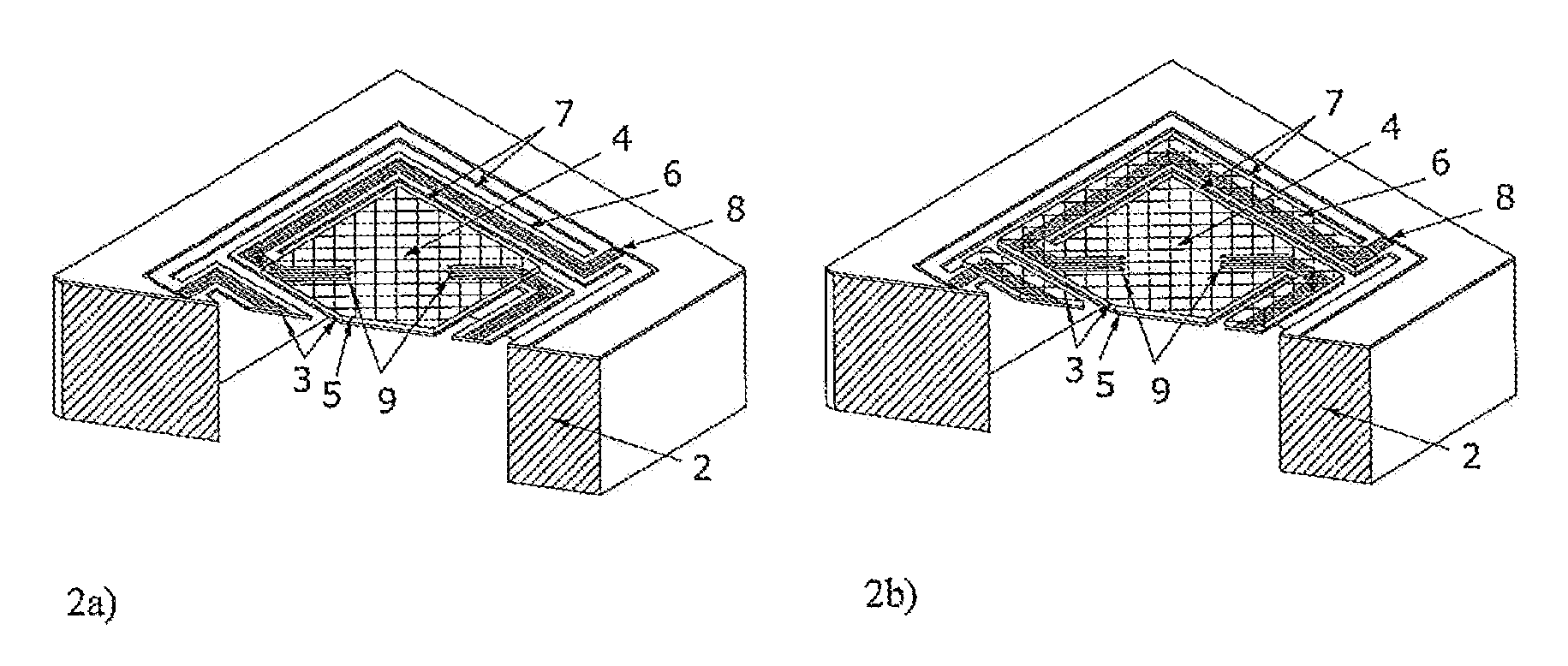
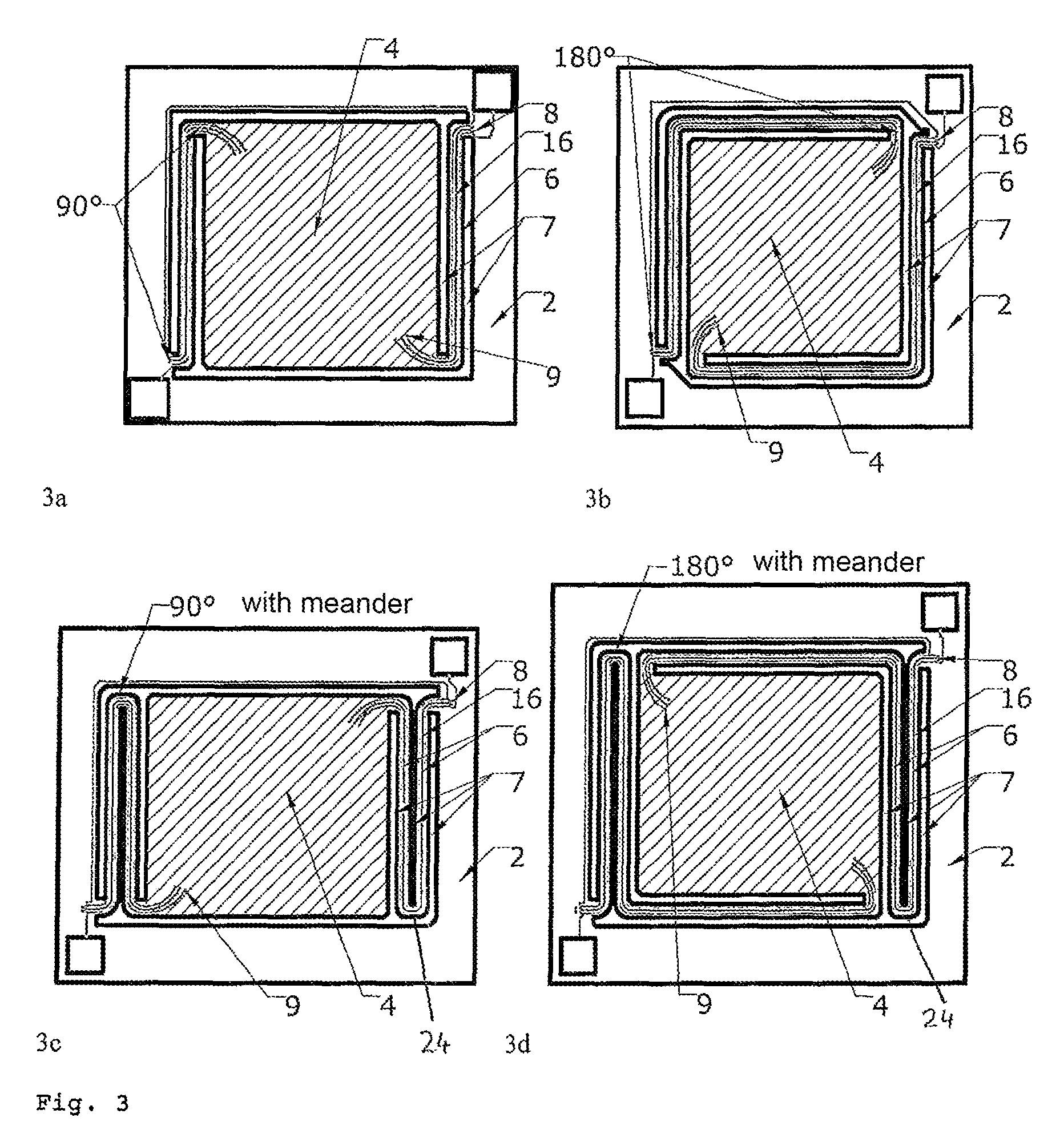
[0097]The choice of embodiment as the vacuum housing or with a gas filling of a gas that is a poor heat conductor also has an effect on the optimization of the sensor chip design. Thus, simulation calculations show that the optimal number of thermoelements when using vacuum housing technology should be very low. Preferably no more than four to eight thermoelements per sensor element should be used in order to achieve a detectivity of the thermopile that is as high as possible. Then these thermoelements are distributed among the number of connecting webs 6 that support the membrane 3.

[0098]If, in contrast, a housing structure with a gas that is a poor heat conductor is chosen, then a higher number of thermoe...


PUM


Abstract

A thermal infrared sensor is provided in a housing with optics and a chip with thermoelements on a membrane. The membrane spans a frame-shaped support body that is a good heat conductor, and the support body has vertical or approximately vertical walls. The thermopile sensor structure consists of a few long thermoelements per sensor cell. The thermoelements being arranged on connecting webs that connect together hot contacts on an absorber layer to cold contacts of the thermoelements. The membrane is suspended by one or more connecting webs and has, on both sides of the long thermoelements, narrow slits that separate the connecting webs from both the central region and also the support body. At least the central region is covered by the absorber layer.

Description

CROSS REFERENCE TO RELATED APPLICATIONS[0001]This application claims priority of German Application No. 10 2010 004 938.7 filed on Jan. 18, 2010 and German Application No. 10 2010 042 108.1 filed on Oct. 7, 2010, which applications are hereby incorporated by reference herein in their entirety.BACKGROUND ART[0002]The invention relates to a thermal infrared sensor in a housing with optics and a chip with thermoelements in the form of thermopile, bolometer or pyroelectric sensor structures on a membrane, which spans a frame-shaped support body that is a good heat conductor, wherein the support body has vertical or approximately vertical walls.[0003]There exist infrared sensors that can be produced in a variety of variants using silicon micromachining technology.[0004]For example, US 2003 / 0054179 A1 introduces a sensor cell for, inter alia, thermopiles, with a thin membrane and an absorber affixed thereon.[0005]The support substrate beneath the sensor structure is mechanically recessed ...

Claims


Application Information

Patent Timeline
Patent Type & Authority Patents(United States)
IPC IPC(8): G01J5/12
CPCG01J5/02G01J5/023G01J5/04G01J5/045G01J5/08G01J5/0853G01J5/10G01J5/12H01L2224/48091H01L2924/00014H01L2924/1461H01L2924/00
Inventor FORG, BODOHERRMANN, FRANKLENEKE, WILHELMSCHIEFERDECKER, JOERGSIMON, MARIONSTORCK, KARLHEINZSCHULZE, MISCHA
Owner HEIMANN SENSOR GMBH
Why Eureka
Try Eureka