Intelligent defect diagnosis method

a defect diagnosis and intelligent technology, applied in the field of diagnostic methods, can solve problems such as the inability to analyze the possible defect failure pattern systematically

Inactive Publication Date: 2013-12-10
ELITETECH TECH
View PDF6 Cites 18 Cited by
  • Summary
  • Abstract
  • Description
  • Claims
  • Application Information

AI Technical Summary

Benefits of technology

[0010]The primary object of present invention is to monitor and debug defect yield in a fabrication process on a near real-time basis; particularly, apply defect data mining technique on automatic defect classification data and defect yield data, image metrology data with fab in-line data to debug defect yield loss or process window quickly.
[0019]Whereby, the intelligent defect diagnosis method may have quick monitoring and rapid debugging defect yield from the fab. Besides, the defect image pattern metrology analysis is to identify systematic defect pattern and process defect pattern. Check metrology data of composite defect image pattern, layout pattern, and lithography simulation pattern polygons whether it is against pattern spec. Moreover, the defect yield prediction data and WIP data provide real-time logistic good die delivery quantity prediction. The frequent failure defect layout pattern analysis uses layout pattern group based defect composite pattern analysis technique to find out major yield killer defect patterns in manufacturing. Last, a powerful defect encyclopedia pattern viewer is built based on image pattern metrology analysis. This full chip manufacturing pattern contour viewer provides the first real manufacturing pattern viewer like a design layout viewer used in design house.

Problems solved by technology

No one analyzes possible defect failure pattern systematically from layout pattern analysis, but from physical failure analysis on failed die or packages.

Method used


Image

  • Intelligent defect diagnosis method
  • Intelligent defect diagnosis method
  • Intelligent defect diagnosis method

Examples


Embodiment Construction

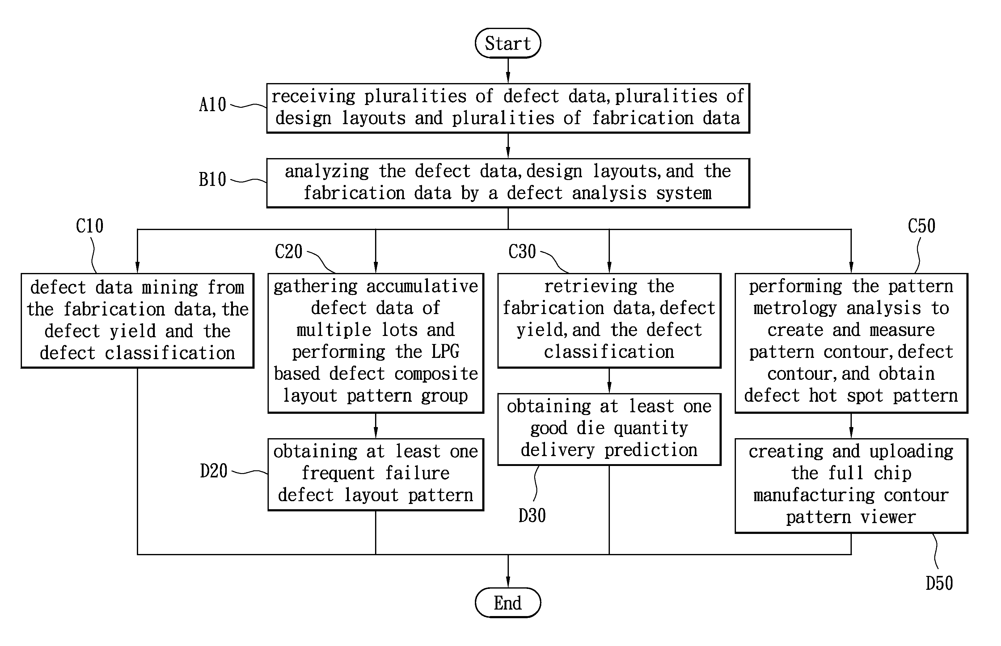
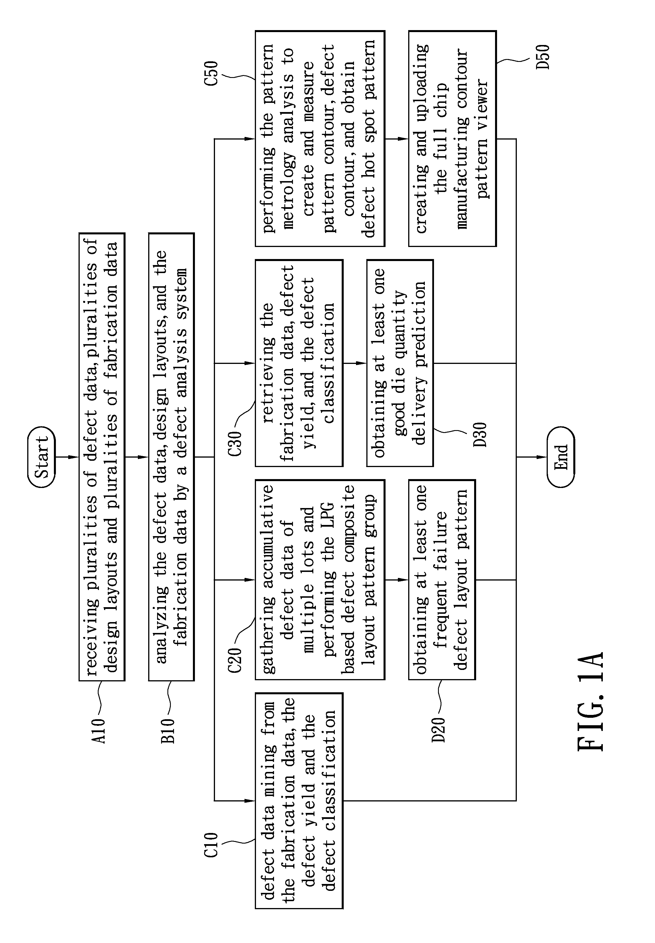
[0032]In manufacturing industry for semiconductor, flat panel, solar cell, Light Emitted Diode (LED) or Printed Circuit Board (PCB) and Assembly mask fab, the defects generated in the manufacturing factory (hereafter referred as fab) are probed and analyzed by all kinds of effort. Those defects in electronic product may be inevitably generated due to nature of the manufacturing process technical limitation or poor control of the equipments. Please refer to FIG. 3A, several facilities such as fab storage unit 91, defect inspection tool 92, storage retrieve unit 93 and defect analysis system 94 are normally utilized in the fab 90 for the purpose of reducing physical deficiencies on the aforementioned products. The fab defect inspection tool 92 and the fab storage unit 91 which obtains and stores up the defect data are normally linked to the storage retrieve unit 93, and so as to further connect to the defect analysis system 94. After the defect data are analyzed by the defect analysis...


PUM


Abstract

An intelligent defect diagnosis method for manufacturing fab is provided. The intelligent defect diagnosis method comprises: receiving pluralities of defect data, design layouts and fabrication data; analyzing the defect data, design layouts, and the fabrication data by a defect analysis system, wherein the analyzing step further contains the sub-steps: segmenting and grouping the design layouts into pluralities of multi-pattern group cells to construct LPG cell based pattern groups; introducing the defect data; segmenting defect image into pluralities of defect and pattern contours; mapping the defect data to each multi-pattern group cell to form the LPG based defect composite pattern group; performing coordinate conversion and pattern match between image contour and design layout for coordinate correction; fulfilling CAA with defect contour, pattern contour and design layout, and obtaining corresponding defect yield; classifying the defect type of defect data through defect image classification analysis.

Description

BACKGROUND OF THE INVENTION[0001]1. Field of the Invention[0002]The present invention relates to a diagnosis method, particularly to a defect diagnosis method for implementation in semiconductor fab, flat panel display fab, solar cell fab, Printed Circuit Board (PCB) mask fab or LED assembly house.[0003]2. Description of Related Art[0004]The sophisticated manufacturing techniques in a fabrication process for integrated circuit dice includes film deposition, masking, photo lithography, etching, etc. During the fabrication process, defects may occur as a result of factors attributed from different sources, for example, equipment malfunction, facility leak, impurities of environment, and design layout problems or the like. These defects can generally be categorized into random defects or systematic defects. Regardless of the form of defect, defects in pattern size may affect the production yield, which in turn will translate into higher cost. In a fab (i.e. manufacturing factory), “Per...

Claims


Application Information

Patent Timeline
Patent Type & Authority Patents(United States)
IPC IPC(8): G06F17/50
CPCG05B19/41875G05B19/00H01L22/12H01L22/20G05B2219/45031G05B2219/37224Y02P90/02
Inventor LEU, IYUN
Owner ELITETECH TECH
Why Eureka
Try Eureka