Method for monitoring quality of an insulation layer

a technology for monitoring the quality of insulation layers, applied in the testing/measurement of individual semiconductor devices, semiconductor/solid-state devices, instruments, etc., can solve the problems of stress-induced degradation of insulation layers, inability to accurately simulate device failures, and various compositions of insulation layers, etc., to achieve accurate simulation of device failures, simple, fast and automated in-line monitors

Inactive Publication Date: 2005-02-24
UNITED MICROELECTRONICS CORP
View PDF2 Cites 20 Cited by
  • Summary
  • Abstract
  • Description
  • Claims
  • Application Information

AI Technical Summary

Benefits of technology

[0020] It is therefore a primary objective of the claimed invention to provide a method for monitoring the quality of an insulation layer, and more particularly, to a method for quickly monitoring the quality of an insulation layer in a device or a structure by measuring the stress-induced leakage current (SILC) with wafer acceptance testing (WAT) equipment.
[0023] It is an advantage of the claimed invention to examine the insulation layer quality in a flash ROM cell, a MOS transistor, a capacitor, or an interconnection structure with a simple, fast, and automated in-line monitor by utilizing the wafer acceptance testing equipment in a clean room and a β− voltage curve. The claimed invention method is very sensitive to the intermediate charges trapped inside the insulation layer and at the interface of the insulation layer and other materials and reflects the real-time change. A swing time-dependent DC ramping voltage is utilized to do the test, which exerts continuous stress fields to the insulation layer. The stress-induced leakage current (SILC) is therefore more readily produced to accurately simulate device failure when compared with the methods adopting single voltage value.

Problems solved by technology

When considering the qualities of MOS transistors, non-volatile memories, capacitors, and interconnect structures, the qualities of the insulation layers, having various compositions, in these devices or structure become important issues.
Actually, the stress-induced degradation of the insulation layer tends to occur, no matter what kind of insulation layer is.
Both the oxide-trapped charges and the interface-trapped charges cause a threshold voltage shift and mobility degradation.
Stress-induced leakage current degrades data retention of non-volatile memories, causes problems during the writing and erasing of non-volatile memories and results in reliability issues.
If the threshold voltage of a MOS transistor is unstable or out of spec, the turn-on and turn-off of the MOS transistor become abnormal and further affect the accuracy of the operation of an integrated circuit.
Electrons captured by those interface traps do not have sufficient time to be thermally emitted and remain captured by the interface traps.
Once the hole barrier is reduced, holes that flow to recombine with the electrons captured by those interface traps do not have sufficient time to be thermally emitted.
If the gate leakage current is greater than a predetermined spec, the quality of the oxide layer is not acceptable.
However, the prior art methods for judging the quality of the oxide layer all have limitations regardless of which method is used, the C-V method, the charge pumping method or to directly measure the gate leakage current.
When compared with other methods, the C-V method requires a MOS capacitor with larger area, is feasible only when the charge quantity is larger than a specific value, and adds to measuring difficulties by using a more complicated equation.
In addition, the C-V method cannot be applied to a production line because the wafer acceptance testing equipment cannot measure capacitance.
Though the method to directly measure the gate leakage current is quite simple, the information obtained is very limited.
In other words, the steps of writing, erasing, and measuring are repeated many times with consuming a large amount of time.

Method used


Image

  • Method for monitoring quality of an insulation layer
  • Method for monitoring quality of an insulation layer
  • Method for monitoring quality of an insulation layer

Examples


Embodiment Construction

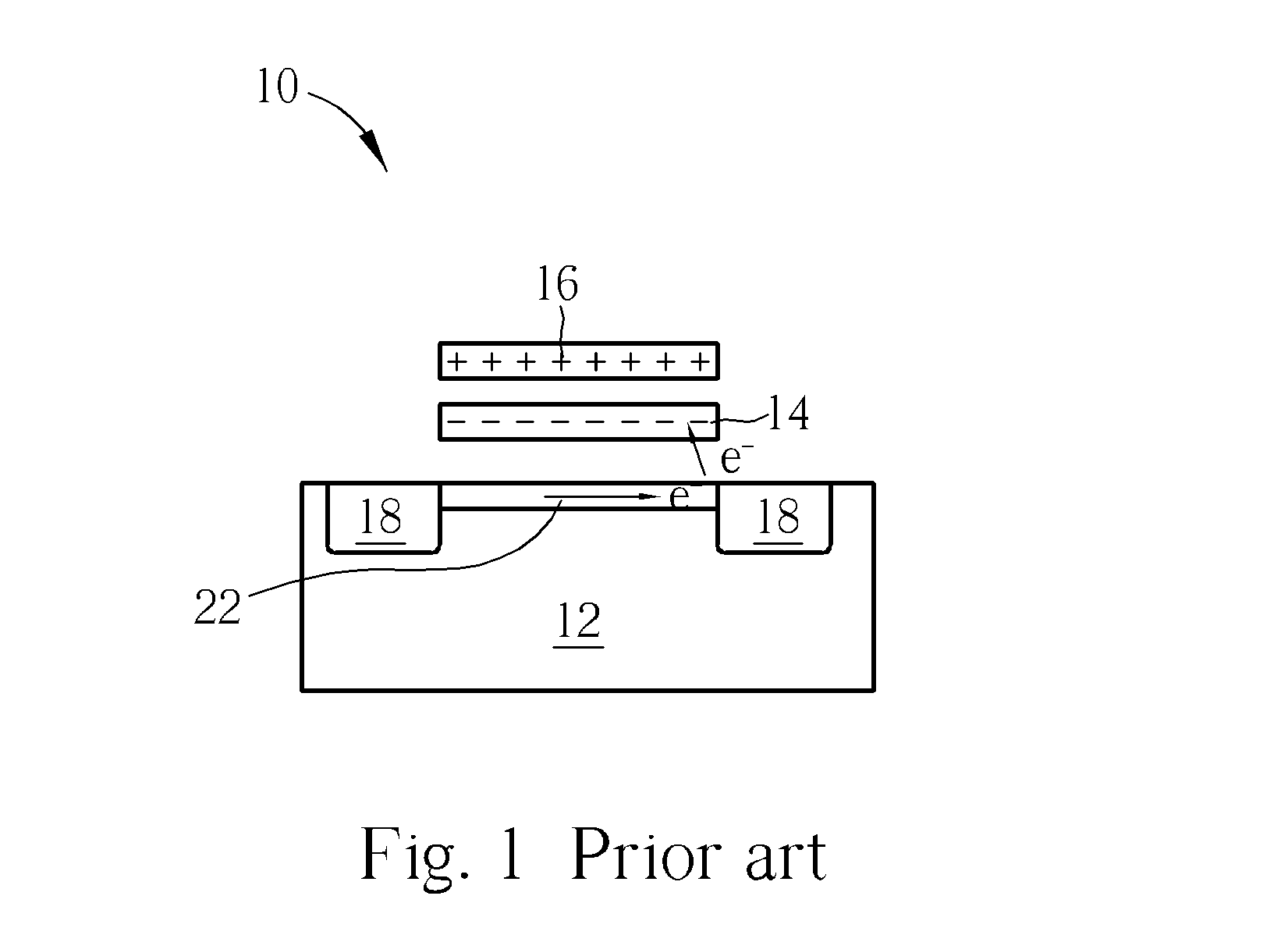
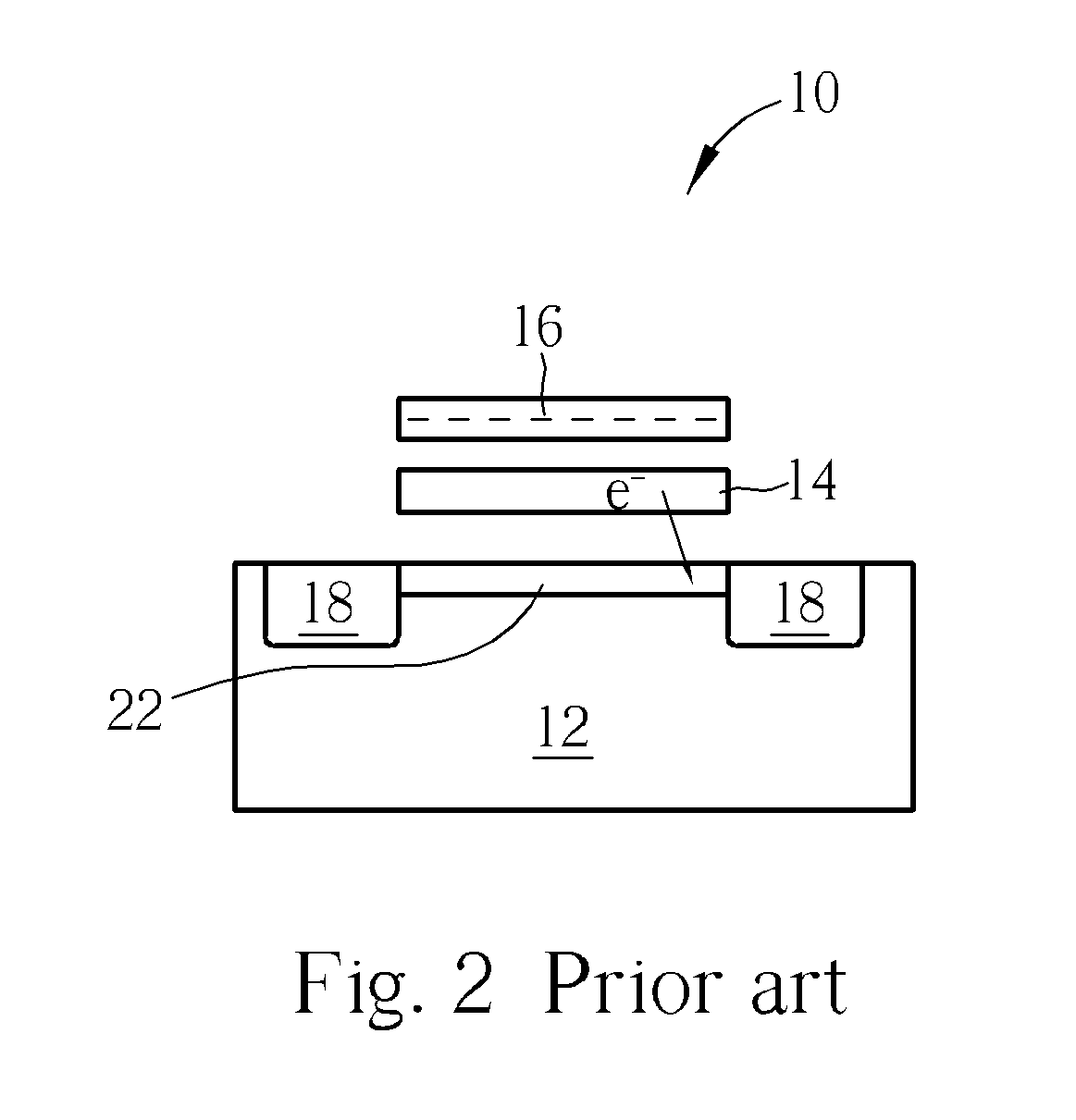
[0038] The principle for monitoring the quality of the insulation layer according to the present invention is to utilize the Fowler-Nordheim tunneling mechanism equation. That means, the method provided by the present invention may be applied to any of the insulation layers in which the Fowler-Nordheim tunneling occur. The insulation layer may be a tunnel oxide layer in a flash memory cell or other non-volatile memory cells, a gate oxide layer in a MOS transistor, a capacitor dielectric layer in a capacitor, or an inter layer dielectric in a interconnection structure. For example, a gate current (Ig) is due to Fowler-Nordheim tunneling when the voltage difference across the oxide layer for the SiO2—Si interface is greater than approximately 3.2V. However, since both the insulation layer and the material layer directly contacting with the insulation layer may have different material compositions, different interfaces are thus formed. The voltage difference across the insulation layer...


PUM


Abstract

The present invention utilizes wafer acceptance testing equipment to fast monitor the quality of an insulation layer. A plurality of swing time-dependent DC ramping voltages are applied to one of the electrode plates in a capacitor and each corresponding leakage current is measured to calculate each corresponding β value. Then, a ratio of each β value is calculated and a β− voltage curve is plotted to actually simulate the device failure.

Description

CROSS REFERENCE To RELATED APPLICATIONS [0001] This is a continuation-in-part of U.S. application Ser. No. 10 / 065,432, filed Oct. 17, 2002, and which is included herein by reference.BACKGROUND OF INVENTION [0002] 1. Field of the Invention [0003] The present invention provides a method for monitoring quality of an insulation layer, and more particularly, relates to a method for quickly monitoring the stress-induced degradation of an insulation layer in different structures with wafer acceptance testing (WAT) equipment. [0004] 2. Description of the Prior Art [0005] In today's electronics industry, semiconductor devices make extensive use of the unique characteristics of semiconductor materials. Most recently, transistors known as metal-oxide-semiconductor (MOS) transistors have been created that consume less power and can be highly integrated. These tiny transistors have been widely used in various electronic devices and circuits. Non-volatile memory, such as the frequently seen flash...

Claims


Application Information

Patent Timeline
Patent Type & Authority Applications(United States)
IPC IPC(8): G01R31/26G01R31/28G11C29/00
CPCG01R31/2648G11C29/006G01R31/2831H01L22/14
Inventor KANG, TING-KUOCHEN, YI-FANKAO, CHIA-JEN
Owner UNITED MICROELECTRONICS CORP
Why Eureka
Try Eureka