Compliant core peripheral lead semiconductor test socket

a technology of peripheral lead and semiconductor, applied in the direction of dielectric characteristics, instruments, printed circuit aspects, etc., can solve the problems of affecting the performance of the circuit board, and affecting the performance of the contact, etc., to achieve excellent electrical performance, reduce the cost of production, and reduce the effect of contact loss

Inactive Publication Date: 2013-12-17
HSIO TECH
View PDF249 Cites 51 Cited by
  • Summary
  • Abstract
  • Description
  • Claims
  • Application Information

AI Technical Summary

Benefits of technology

[0014]The present disclosure is aimed at a test socket that is inexpensive to produce, has relative long life and provides excellent electrical performance.

Problems solved by technology

A socket with good electrical performance is critical for many IC testing functions since poor performance can result in retesting or discarding devices that are actually acceptable but failed the test due to degradation within the socket.
In general, they all have a range of mechanical life that is limited by the effects of contacting the solder that is plated onto the terminals of the IC device.
As the solder collects on the tips of the contacts, the Tin within the solder oxidizes to form a high resistance layer that causes the contact to lose electrical performance.
This movement can cause wear on the PCB which can degrade performance of the circuit board.
In general, the need for thousands of cycles before replacement drives sophisticated design that can be expensive.
The socket volumes can also be relatively small requiring custom production methods that can also be expensive.
The methods used to produce the plastic socket housings which hold the contacts are typically expensive precision machining operations.
Those sockets that can pass the electrical performance requirements can be limited by cost or the amount of use before they must be repaired or replaced.
It can take hours or days to replace the failing socket, with the corresponding unit volume of IC devices which could have been tested being a major factor in the overall cost of use (e.g., an opportunity cost).
Damage to the PCB used for the test interface can also dramatically impact the cost of use as the PCB's can be very expensive and have a long lead-time to build (and replace).
Traditional IC sockets have reached an electrical performance limit.
Next generation IC devices will operate above 5 GHz and beyond and the existing IC sockets do not provide acceptable performance levels without significant revision.

Method used


Image

  • Compliant core peripheral lead semiconductor test socket
  • Compliant core peripheral lead semiconductor test socket
  • Compliant core peripheral lead semiconductor test socket

Examples


Embodiment Construction

[0046]A high performance electrical interconnect according to the present disclosure may permit fine contact-to-contact spacing (pitch) on the order of less than 1.0 mm pitch, and more preferably a pitch of less than about 0.7 millimeter, and most preferably a pitch of less than about 0.4 millimeter. Such fine pitch high performance electrical interconnects are especially useful for communications, wireless, and memory devices.

[0047]The present high performance electrical interconnect can be configured as a low cost, high signal performance interconnect assembly, which has a low profile that is particularly useful for desktop and mobile PC applications. IC devices can be installed and uninstalled without the need to reflow solder. The solder-free electrical connection of the IC devices is environmentally friendly.

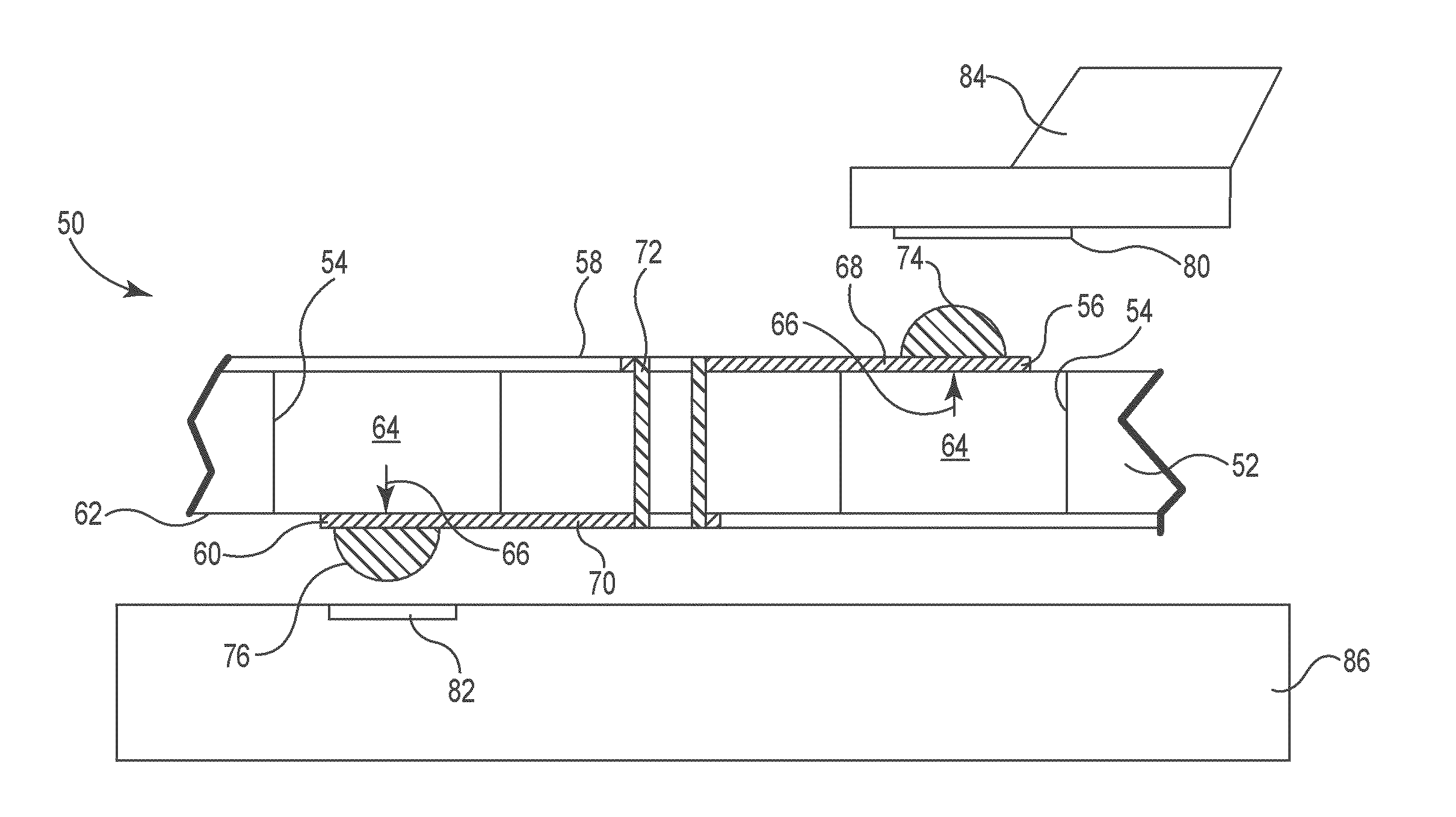
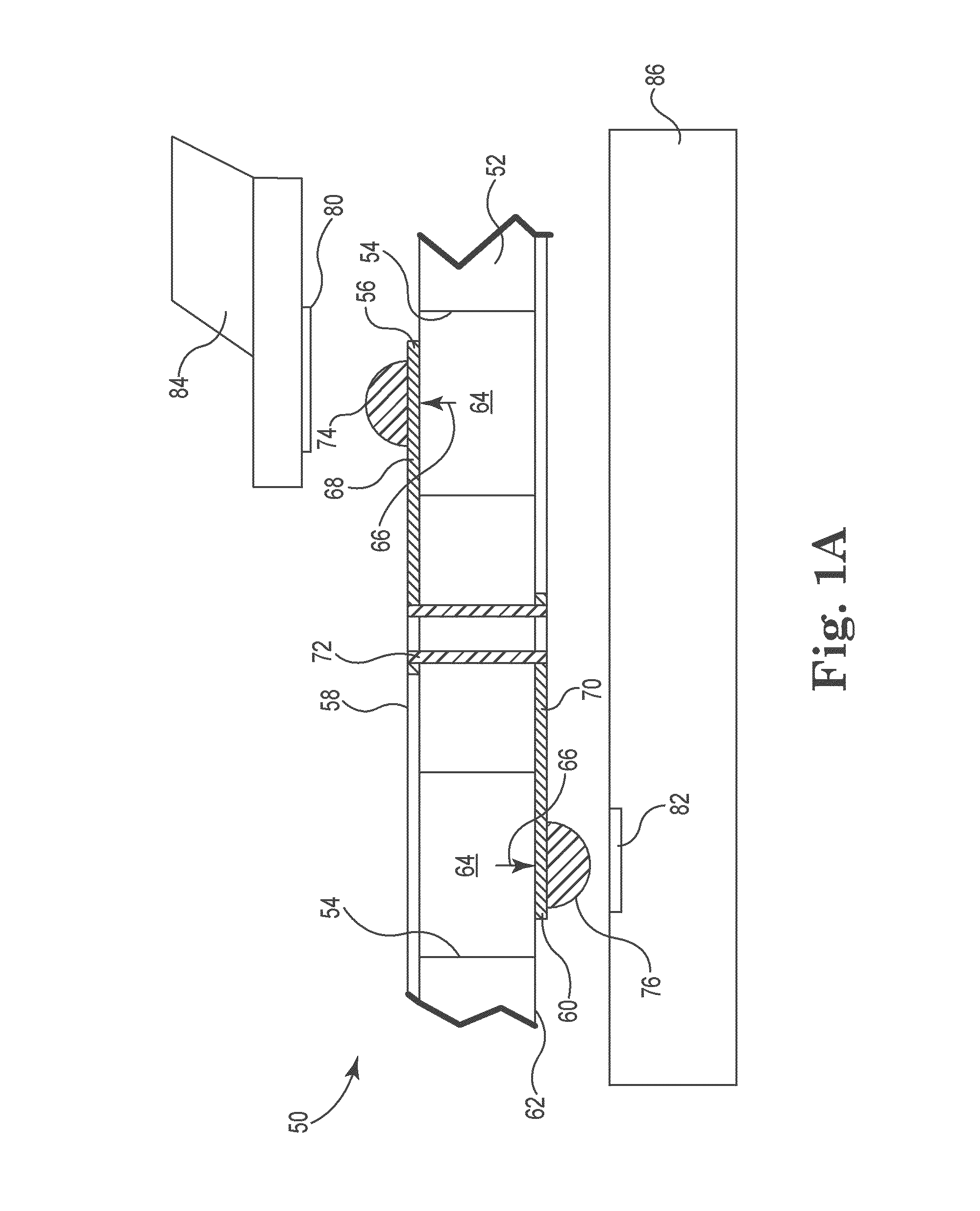
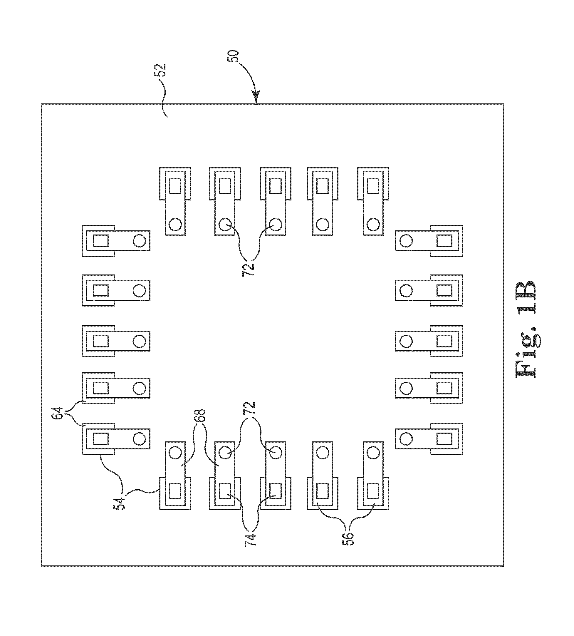
[0048]FIG. 1A is a side sectional view of an electrical interconnect 50 for a semiconductor test socket in accordance with an embodiment of the present disclosure. Core mat...


PUM

PropertyMeasurementUnit
thickaaaaaaaaaa
aspect ratioaaaaaaaaaa

Abstract

An electrical interconnect for providing a temporary interconnect between terminals on an IC device and contact pads on a printed circuit board (PCB). The electrical interconnect includes a substrate with a first surface having a plurality of openings arranged to correspond to the terminals on the IC device. A compliant material is located in the openings. A plurality of conductive traces extend along the first surface of the substrate and onto the compliant material. The compliant material provides a biasing force that resists flexure of the conductive traces into the openings. Conductive structures are electrically coupled to the conductive traces over the openings. The conductive structures are adapted to enhance electrical coupling with the terminals on the IC device. Vias electrically extending through the substrate couple the conductive traces to PCB terminals located proximate a second surface of the substrate.

Description

RELATED APPLICATIONS[0001]This application claims the benefit of U.S. Provisional Application No. 61 / 476,504, filed Apr. 18, 2011, the disclosure of which is hereby incorporated by reference.[0002]This application is a continuation-in-part of U.S. patent application Ser. No. 13 / 266,573, titled COMPLIANT PRINTED CIRCUIT AREA ARRAY SEMICONDUCTOR DEVICE PACKAGE, filed Oct. 27, 2011, which is a national stage application under 35 U.S.C. §371 of International Application No. PCT / US2010 / 036363, titled COMPLIANT PRINTED CIRCUIT AREA ARRAY SEMICONDUCTOR DEVICE PACKAGE, filed May 27, 2010, which claims priority to U.S. Provisional Application No. 61 / 183,411, filed Jun. 2, 2009, all of which are hereby incorporated by reference in their entireties.[0003]This application is a continuation-in-part of U.S. patent application Ser. No. 13 / 318,382, entitled RESILIENT CONDUCTIVE ELECTRICAL INTERCONNECT, filed Oct. 1, 2011, which is a national stage application under 35 U.S.C. §371 of International A...

Claims


Application Information

Patent Timeline
Patent Type & Authority Patents(United States)
IPC IPC(8): H01L23/34
CPCG01R1/0416H05K3/4007H01L23/522H05K3/325H05K2201/0133H05K2201/0187H05K2201/09036Y10T29/49165H05K2201/0949H05K2201/10378H05K2203/162H01L2224/13H05K2201/09481H01L23/34
Inventor RATHBURN, JAMES
Owner HSIO TECH
Why Eureka
Try Eureka