Method of tailoring conformality of Si-containing film

a conformality and film technology, applied in the field of tailoring conformality of si-containing films, can solve problems such as the difficulty of controlling and achieve the effect of improving the conformality of films

Active Publication Date: 2014-03-11
ASM JAPAN
View PDF10 Cites 439 Cited by
  • Summary
  • Abstract
  • Description
  • Claims
  • Application Information

AI Technical Summary

Problems solved by technology

In some embodiments, the film is a silicon nitride film for which it is typically difficult to control its conformality even if applied RF power is pulsed.

Method used


Image

  • Method of tailoring conformality of Si-containing film
  • Method of tailoring conformality of Si-containing film
  • Method of tailoring conformality of Si-containing film

Examples


example 1

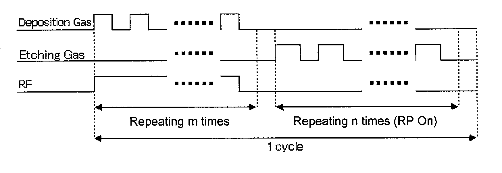
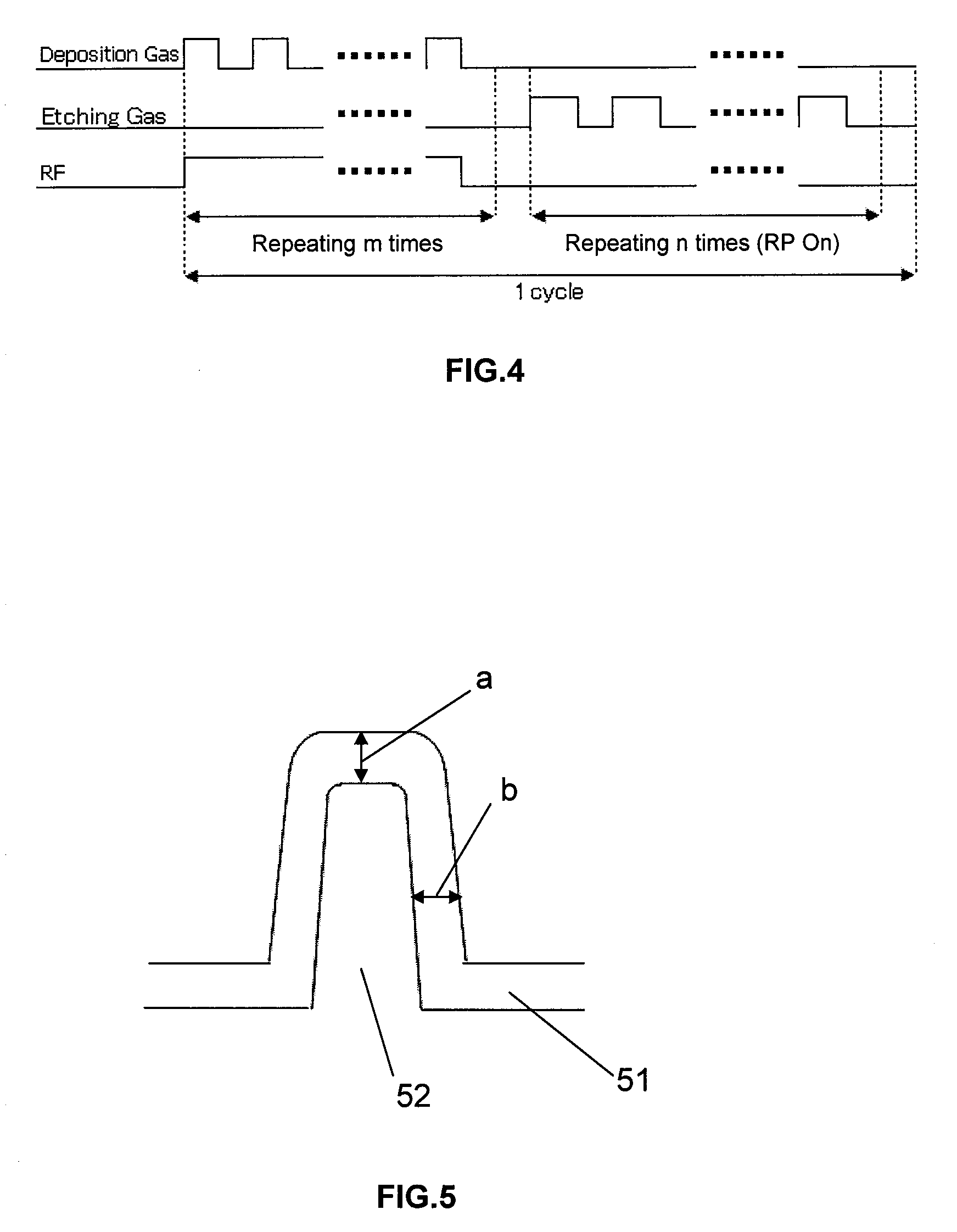
[0061]A silicon nitride film was formed on a substrate having trenches under the conditions shown below using the sequence illustrated in FIG. 4 and the PEALD apparatus illustrated in FIG. 6. The trenches included relatively wide trenches (a width of 500 nm and a depth of 350 nm) and relatively narrow trenches (a width of 50 nm and a depth of 350 nm). Thus trenches of different aspect ratio were coated.

[0062]Deposition Session

[0063]Trisilyamin (TSA): 300 sccm

[0064]Hexane: 300 sccm

[0065]Hydrogen: 500 sccm

[0066]Nitrogen: 50 sccm

[0067]Argon: 1000 sccm

[0068]Helium: 1400 sccm

[0069]Substrate Temp.: 400° C.

[0070]RF power (a frequency of 13.56 MHz): 50 W (0.07 W / cm2)

[0071]Pressure: 500 Pa

[0072]Deposition gas (TSA+hexane) supply time: 0.3 sec supply, 2 sec purge

[0073]Number of cycles in one session of deposition: 180

[0074]Etching Session (Remote Plasma)

[0075]Argon: 4000 sccm

[0076]NF3: 20 sccm

[0077]Pressure: 520 Pa

[0078]Etching gas supply time: 6 sec supply, 6 sec purge

[0079]As illustrated in...

example 2

[0089]Using the same apparatus and process conditions as in Example 1 except that the NF3 gas flow was 40 sccm, and the etching duration (etching gas flow step) was 3 seconds and 4 seconds, a film was formed. The top / side etching ratio was as follows:

[0090]

TABLE 3etching time3 sec4 secTop / Side etching4.91.8ratio

[0091]It was confirmed that the shorter the etching time, the higher the top / side etching ratio became. Thus, by adjusting the duration of etching, it is possible to obtain a film having high conformality.

example 3

[0092]Using the same apparatus as in Example 1 except that NF3 gas was introduced without activating the remote plasma unit into the reaction chamber, and then was excited using RF power applied in the reaction chamber, a silicon nitride film was formed on a substrate. The etching conditions were as follows: Ar flow: 4000 sccm, NF3 flow: 5 to 50 sccm, and RF power: 20 to 100 W.

[0093]After the deposition, etching was conducted once for 6 seconds, 10 seconds, and 15 seconds. The top / side etching ratio was determined as follows:

[0094]

TABLE 4etching time6 sec10 sec15 secTop / Side etching2.2521.1ratio(2.7 nm / 1.2 nm)

[0095]It was confirmed that the shorter the etching time, the higher the top / side etching ratio became. Thus, by adjusting the duration of etching, it is possible to obtain a film having high conformality.


PUM

PropertyMeasurementUnit
thicknessaaaaaaaaaa
thicknessaaaaaaaaaa
thicknessaaaaaaaaaa

Abstract

A method of tailoring conformality of a film deposited on a patterned surface includes: (I) depositing a film by PEALD or pulsed PECVD on the patterned surface; (II) etching the film, wherein the etching is conducted in a pulse or pulses, wherein a ratio of an etching rate of the film on a top surface and that of the film on side walls of the patterns is controlled as a function of the etching pulse duration and the number of etching pulses to increase a conformality of the film; and (III) repeating (I) and (II) to satisfy a target film thickness.

Description

BACKGROUND OF THE INVENTION[0001]1. Field of the Invention[0002]The present invention generally relates to pulsed plasma enhanced chemical vapor deposition (PPECVD) and plasma enhanced atomic layer deposition (PEALD) for depositing conformality-tailored films.[0003]2. Description of the Related Art[0004]PPECVD / PEALD processes can provide high conformality (also referred to as “coverage”) of films depositing on a patterned surface on which multiple recesses or grooves are formed in patterns for establishing interconnects, as compared with plasma enhanced chemical vapor deposition (PECVD) processes. However, PEALD processes are typically not as good as thermal ALD in terms of conformality, although PEALD processes are typically better than thermal ALD in terms of deposition rates and controllability, depending on the type of films.[0005]High conformality refers to a high ratio of a thickness of film deposited on a side wall of a recess to a thickness of film deposited on a top surface...

Claims


Application Information

Patent Timeline
Patent Type & Authority Patents(United States)
IPC IPC(8): H01L21/311H01L21/302C23C16/00H01L21/31
CPCH01L21/0228C23C16/45523H01L21/0217H01L21/02167C23C16/345H01L21/02274
Inventor ONIZAWA, SHIGEYUKILEE, WOO-JINFUKUDA, HIDEAKINAMBA, KUNITOSHI
Owner ASM JAPAN
Why Eureka
Try Eureka