
Organic electronic device comprising an organic semiconducting material

a semiconducting material and electronic device technology, applied in the field of organic electronic devices comprising organic semiconducting materials, can solve the problems of reducing contact resistance, less common methods, and difficulty in determining electron affinity, and achieve good lumo position for organic light-emitting, good conductivity and charge carrier mobility, and high thermal stability

Active Publication Date: 2014-04-01
NOVALED GMBH
View PDF23 Cites 7 Cited by
  • Summary
  • Abstract
  • Description
  • Claims
  • Application Information

AI Technical Summary

Benefits of technology

[0062]The compounds can be used as hole blocking layers. Advantageous effects are seen over the prior art since the materials have a higher glass transition temperature compared to materials described in the prior art, such as in DE 10 2007 012 794 or EP 07 400 033.2 (not published yet).
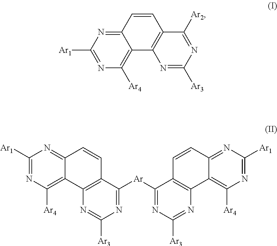
[0063]The use of the compounds according to formula (I)-(II) provides high thermal stability, especially due to high glass transition temperature, a good LUMO position for organic light-emitting devices, good dupability, conductivity and charge carrier mobility, high transparency, easy synthesis. Further, preparation of these compounds can be conducted in a very cost-effective manner.
[0064]It was surprisingly round that especially the thermal stability of doped layers comprising a compound as disclosed can be significantly increased in the devices according to the present invention comprising matrix material. Especially, a glass transition temperature of over 100° C. was achieved with the compound shown in the examples. The combination of such a high glass temperature, the wide gap and the dopability make those compounds to have a high industrial relevance for use in organic electronic devices.
[0065]Additional features and advantages of the invention can be taken from the following detailed description of preferred embodiments, together with the drawings as attached.
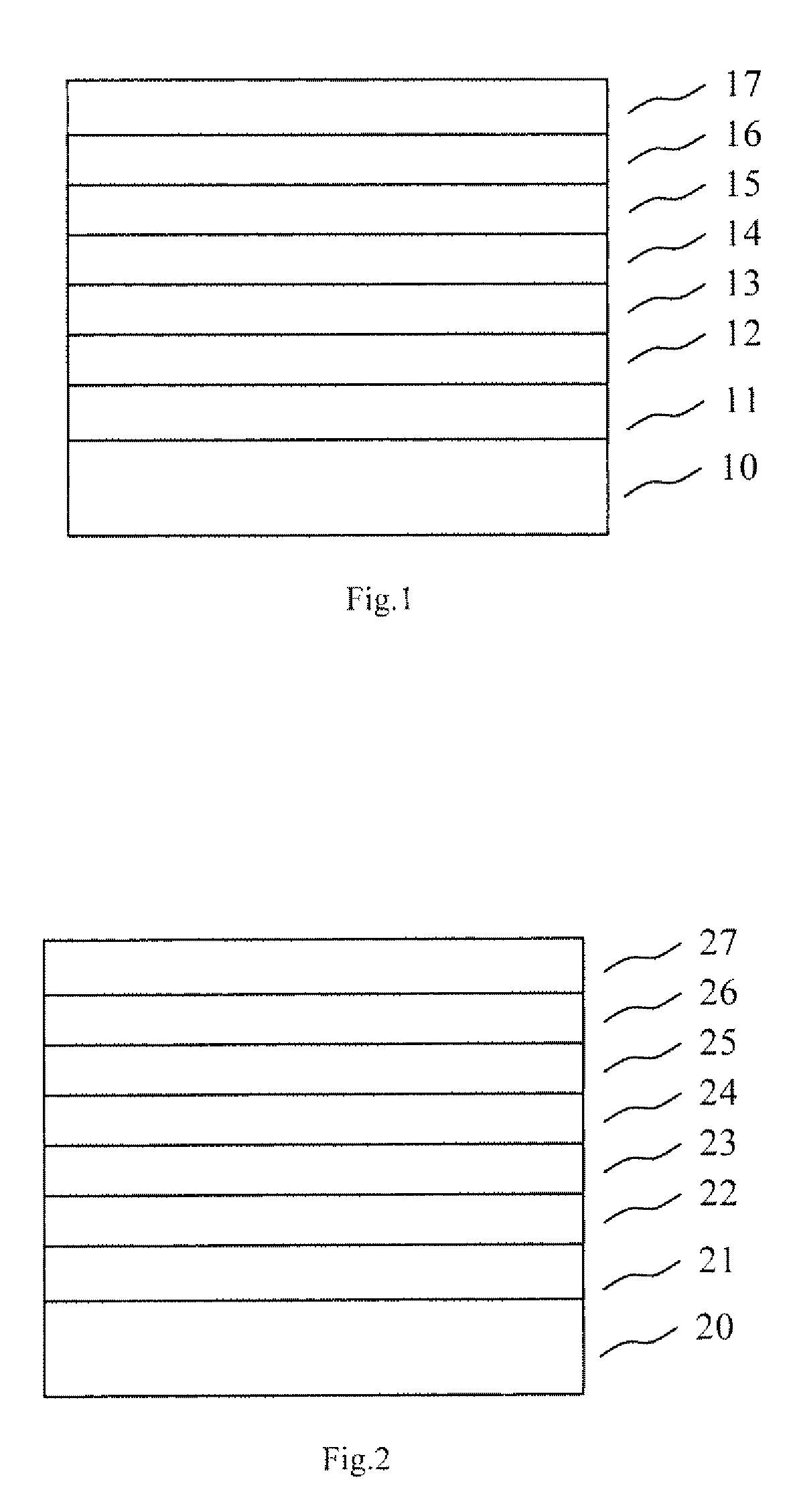
[0066]The organic electronic device of the present invention may be an organic light emitting diode. FIG. 1 shows a typical layer structure of an organic light emitting diode. The layers are disposed on a substrate (10) in the following order: anode (11), p-doped hole transport layer (12), electron blocking layer (13), emission layer (14), hole blocking layer (15), n-electron transport layer (16), and cathode (17). Two or more layers can collapse into a smaller number of layers if properties can be combined. Inverted structure and multiple stacked OLEDs are also well known in the field. The emission layer is usually composed by an emitter matrix material and an emitter dopant; this layer can be also composed by several other layers to generate light with a broad spectrum combining several emitters, for example, to generate white light.
[0067]FIG. 2 shows a typical small molecule organic solar cell. Many variations are possible. One simple structure that offers reasonable efficiencies is composed by a substrate (20), followed by: anode (21), p-doped hole transport layer (22), thin interlayer that is non-doped (23), the photo-active bulk-heterojunction (24), and electron transport layer (25), a buffer layer (26), and the cathode (27).EXAMPLESGeneral Synthesis Method

Problems solved by technology

However, this method is less common.
The reason for that is the difficulty of the determination of the electron affinity.
In the case of light-emitting diodes, the ohmic losses in the charge transport layers during operation are associated with their conductivity.
Furthermore, depending on the charge carrier concentration in the organic layers, bending of the band in the vicinity of a metal contact results which simplifies the injection of charge carriers and can therefore reduce the contact resistance.
Additionally, analogous to the experience with inorganic semiconductors, applications can be anticipated which are precisely based on the use of p- and n-doped layers in a component and otherwise would be not conceivable.
There is a technical challenge to provide electron transport materials (ETM) and emitter host (EMH) materials that have a sufficiently low laying LUMO level so that they can be doped, and still have a high enough laying LUMO level which can efficiently transfer charge to emitter host (in case of an ETM) and transfer energy to the emitter dopant (in case of EMH).
The limitation for high laying LUMO level of the ETL is given by the dopability, since the n-dopants with very high HOMO tend to be unstable; also the injection is difficult for very high LUMO of the ETL.

Method used


Image

  • Organic electronic device comprising an organic semiconducting material
  • Organic electronic device comprising an organic semiconducting material
  • Organic electronic device comprising an organic semiconducting material

Examples


example 1

Synthesis of

[0073]

[0074]First step: Synthesis of 2-phenyl-7,8-dihydroquinazolin-5(6H)-one (1). All manipulations were carried out in air, without any further purification of commercial solvents / chemicals.

[0075]

2-((dimethylamino)methylene)cyclo-16.7 g (100 mmol)hexane-1,3-dioneBenzamidinium Hydrochloride19.2 g (110 mmol)N-ethyl-N-isopropylpropan-2-amine20 mL (120 mmol)Ethanol100 mL

[0076]A suspension of 2-((dimethylamino)methylene)cyclohexane-1,3-dione (16.7 g) and benzamidinium hydrochloride (19.2 g) in 75 mL Ethanol is refluxed in a 250 mL 2 neck-flask equipped with a reflux condenser and a dropwise addition funnel. The suspension turns into a solution upon boiling, after what a solution of N-Ethyl-N-isopropylpropane-2-amine in 25 mL Ethanol is added dropwise within 20 min. The solution turns from yellow to orange and is heated at reflux for 3 hours. The reaction mixture is cooled down to room temperature during which time a thick yellow precipitate appears.

Work Up

[0077]The suspensi...

example 2

Synthesis of

[0105]

[0106]First step: Synthesis of 2-phenyl-7,8-dihydroquinazolin-5(6H)-one (1). All manipulations were carried out in air, without any further purification of commercial solvents / chemicals.

[0107]

2-((Dimethylamino)methylene)16.7 g (100 mmol)cyclohexane-1,3-dioneBenzamidinium Hydrochloride19.2 g (110 mmol)N-ethyl-N-isopropylpropan-2-amine20 mL (120 mmol)Ethanol100 mL

[0108]A suspension of 2-((dimethylamino)methylene)cyclohexane-1,3-dione (16.7 g) and benzamidinium hydrochloride (19.2 g) in 75 mL ethanol is refluxed in a 250 mL 2 neck-flask equipped with a reflux condenser and a dropwise addition funnel. The suspension turns into a solution upon boiling, after what a solution of N-ethyl-N-isopropylpropane-2-amine in 25 mL ethanol is added dropwise within 20 min. The solution turns from yellow to orange and is heated at reflux for 3 hours. The reaction mixture is cooled down to room temperature during which time a thick yellow precipitate appears.

Work Up

[0109]The suspensio...

example 3

Synthesis of

[0135]

[0136]First step: Synthesis of 2-(naphthalen-1-yl)-7,8-dihydroquinazolin-5(6H)-one (7). All manipulations were carried out in air, without any further purification of commercial solvents / chemicals.

[0137]

2-((Dimethylamino)methylene)cyclohexane-1,3-dione16.7 g (100 mmol)Benzamidinium Hydrochloride19.2 g (110 mmol)N-ethyl-N-isopropylpropan-2-amine20 mL (120 mmol)Ethanol100 mL

[0138]A suspension of 2-((dimethylamino)methylene)cyclohexane-1,3-dione (16.7 g) and benzamidinium hydrochloride (19.2 g) in 75 mL ethanol is refluxed in a 250 mL 2 neck-flask equipped with a reflux condenser and a dropwise addition funnel. The suspension turns into a solution upon boiling, after what a solution of N-ethyl-N-isopropylpropane-2-amine in 25 mL ethanol is added dropwise within 20 min. The solution turns from yellow to orange and is heated at reflux for 3 hours. The reaction mixture is cooled down to room temperature during which time a thick yellow precipitate appears.

Work Up

[0139]Th...


PUM

PropertyMeasurementUnit
polarization energyaaaaaaaaaa
LUMOaaaaaaaaaa
LUMOaaaaaaaaaa

Abstract

The present invention relates to organic electronic devices that include an organic semiconducting material. The organic electronic devices may include organic light-emitting diodes, field-effect transistors, sensors, photodetectors, organic solar cells, organic thin-film transistors, organic integrated circuits, organic field-quench devices, organic light-emitting transistors, light-emitting electrochemical cells, or organic laser diodes.

Description

CROSS-REFERENCE TO RELATED APPLICATIONS[0001]This is a submission pursuant to 35 U.S.C. 154(d)(4) to enter the national stage under 35 U.S.C. 371 for PCT / EP2010 / 007081, filed Nov. 23, 2010. Priority is claimed under 35 U.S.C. 119(a) and 35 U.S.C. 365(b) to European Patent Application Number 09 014 598.8, filed. Nov. 24, 2009.[0002]The subject matters of international application no. PCT / EP2010 / 007081 is expressly incorporated herein by reference.FIELD OF THE INVENTION[0003]The present invention relates to an organic electronic device comprising an organic semiconducting material.BACKGROUND OF THE INVENTION[0004]Conjugated organic compounds have different applications. One important field comprises organic semiconductors. Organic semiconductors can be used to fabricate simple electronic components e.g. resistors, diodes, field effect transistors, and also optoelectronic components like organic light emitting devices (e.g. OLED), solar cells, and many others. Non-volatile and volatile...

Claims


Application Information

Patent Timeline
Patent Type & Authority Patents(United States)
IPC IPC(8): C07D487/02
CPCH01L51/42H01L51/5048H01L51/5052Y02E10/549H01L51/0508H01L51/0072Y02P70/50H10K10/46H10K85/6572H10K50/155H10K50/165H10K50/14H10K30/50H10K50/11H10K30/00
Inventor LUX, ANDREAFADHEL, OMRANESALBECK, JOSEFKUSSLER, MANFRED
Owner NOVALED GMBH
Learn More