Inductive antenna coupling

a technology of inductive antennas and couplings, applied in the direction of burglar alarm mechanical actuation, burglar alarm by hand-portable articles removal, instruments, etc., can solve the problems of inability to match the miniaturization exhibited in ics (integrated circuits), and the radiation elements (antennas) needed to radiate information to the outside world remain relatively large, so as to achieve accurate bandwidth prediction, efficiency and performance, the effect of great potential and promis

Active Publication Date: 2014-04-29
TAGARRAY
View PDF7 Cites 9 Cited by
  • Summary
  • Abstract
  • Description
  • Claims
  • Application Information

AI Technical Summary

Benefits of technology

[0009]When a circuit, typically a Silicon chip, is to be connected to one or multiple antennas, the connection mechanism plays an important role. The chip pads are typically very small in size; attaching such pads to external antennas or intermediary antenna interfaces imposes a high degree of accuracy and precision on the attach process. This invention makes it possible to couple a radio chip to external antennas or antenna frontends with low requirements on precision and accuracy and thereby cost.
[0028]Accurate inductor wire layout on chip as well as on the antenna substrate will allow for accurate prediction of bandwidth, efficiency and performance, assigning the bulk of the performance deviation budget to placement inaccuracies.

Problems solved by technology

As the limits of miniaturization in electronic devices are yet to be discovered, the sizes of some other elements in electronics remain constrained by the rules of physics and cannot match the miniaturization exhibited in ICs (Integrated Circuits).
However, the radiation elements (antennas) needed to radiate the information to the outside world remain relatively large.
This mismatch in miniaturization means that extremely small IC pads are to be connected to relatively much larger antennas.
That is, the assembly accuracy is dictated by the IC pad geometry which in turn results in the requirement for high placement accuracy and subsequently high cost of assembly.
The circuitry needed for ESD protection has an undesirable performance impact on an ultra low power radio and in particular on the power recovery frontend of a RFID chip.
This is also true for many high data rate ICs for wireless standards to the extent that in some cases ESD is eliminated altogether from critical signals rendering the system vulnerable to discharge effects.
Coupling media (often bond-wires) tend to result in non-predictable or performance degrading characteristics especially for high frequency applications where the inductance of the coupler becomes an important factor.
Normally, it is very difficult to massively probe and test whole wafers while individual dice are still on them.

Method used


Image

  • Inductive antenna coupling
  • Inductive antenna coupling
  • Inductive antenna coupling

Examples


Embodiment Construction

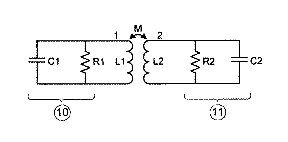
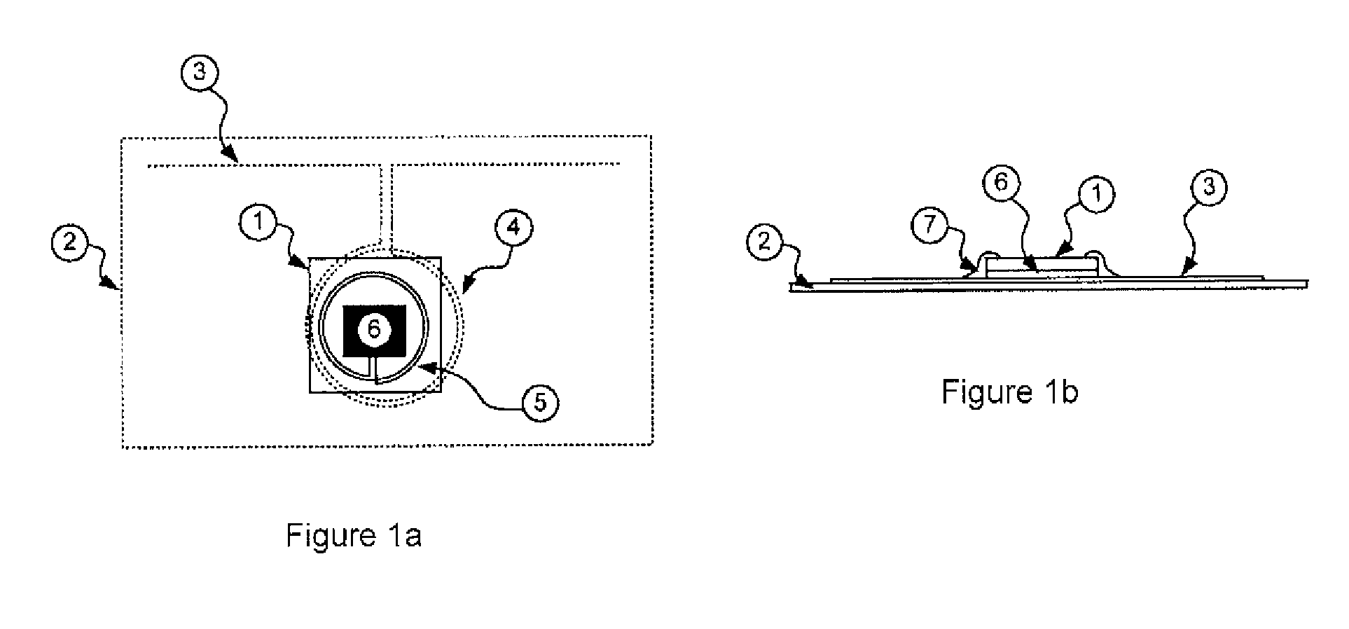
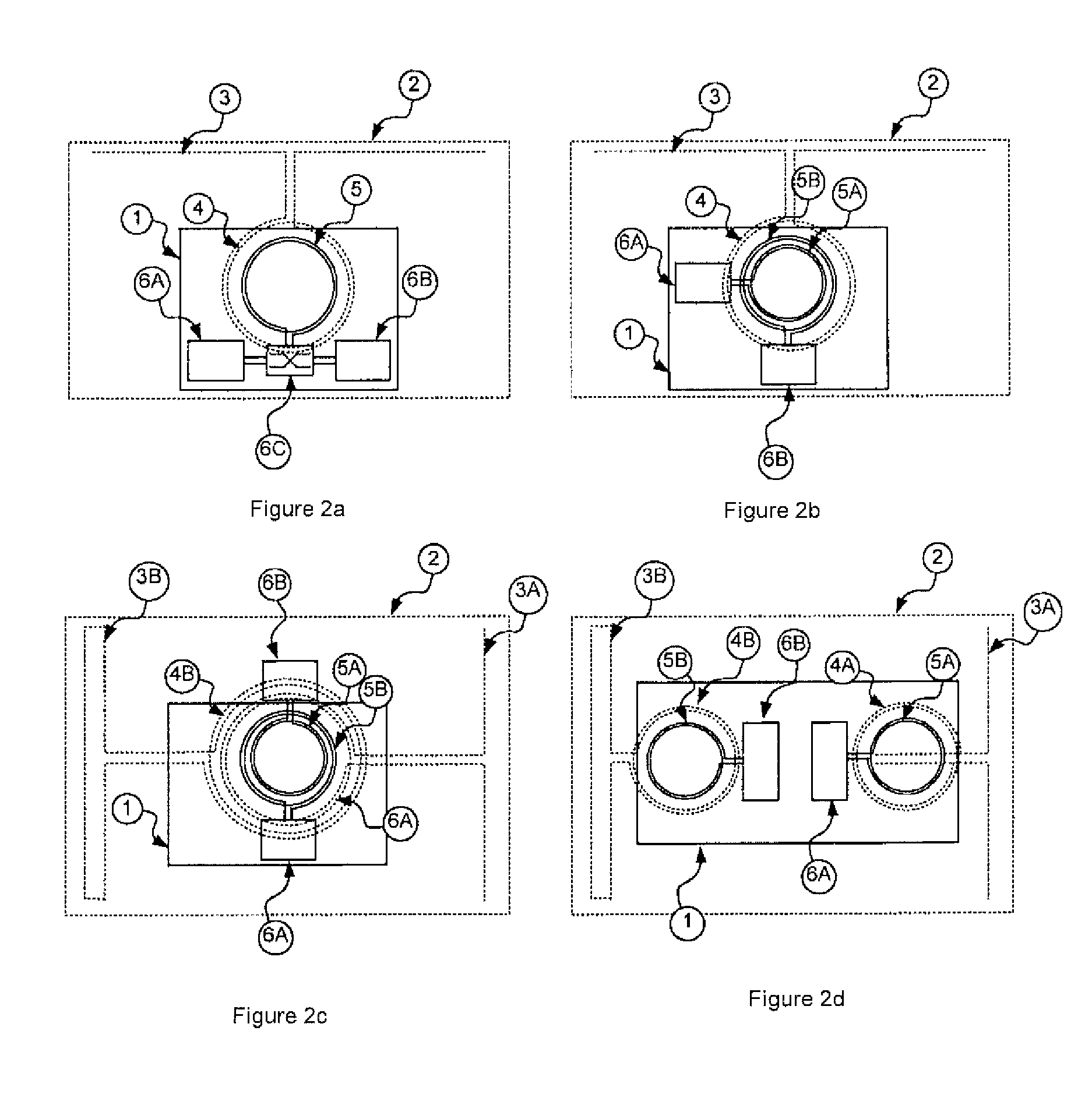
[0041]The invention consists of a transformer with the primary winding on the circuit substrate and the secondary winding on the antenna substrate. The primary side on the chip can use a single turn or multiple turns. It can be implemented in a single planar layer or in multiple layers on any available metal / conductive layers in the process technology. Multiple turns on multiple layers can be used to enhance the inductance. Any combination of the mentioned methods on both sides is possible. The planar inductor could take the form of a polygon spiral shape with multiple sides (including but not limited to 4, 6 and 8 sides) or a circular shape as provided and constrained by the foundry process.

[0042]The diameter size, number of turns, and the width of each turn (no uniform width / thickness of conductor across different turns and / or layers is assumed) are to be optimized for the required frequency and bandwidth in terms of efficiency and impedance transfer. Depending on the substrate fa...


PUM


Abstract

This invention pertains to the connection between a radio frequency circuit and its antenna. Miniaturization of radio frequency integrated circuits has made attaching these circuits to their antennas increasingly difficult and costly. This invention uses magnetic coupling, as performed in transformers, between circuits and antennas as a practical solution to reduce cost and effort in attaching the two sides as well as to protect the circuit against electrostatic discharge. Furthermore a simple pre-assembly testing methodology is accounted for as an additional benefit of the method.

Description

CROSS-REFERENCE TO RELATED APPLICATIONS[0001]N / ASTATEMENT REGARDING FEDERALLY SPONSORED RESEARCH OR DEVELOPMENT[0002]N / ABACKGROUND OF THE INVENTION[0003]This invention relates generally to communication between physical objects, communication and radio systems, radio frequency for item and inventory identification, tracking and management; and more particularly to methods and means of connecting radio circuits and devices to external radiation elements so as to propagate their radio waves.[0004]As the limits of miniaturization in electronic devices are yet to be discovered, the sizes of some other elements in electronics remain constrained by the rules of physics and cannot match the miniaturization exhibited in ICs (Integrated Circuits). A good example of this mismatch in miniaturization is in Radio Frequency Identification (RFID) tags where the whole electric circuit including the memory, controller, radio frequency links, etc. can be implemented in a miniaturized IC, the size of ...

Claims


Application Information

Patent Timeline
Patent Type & Authority Patents(United States)
IPC IPC(8): H04B7/00
CPCG06K19/07749
Inventor PAHLAVAN, KOUROSHARBABIAN, MOHAMMAD AMIN
Owner TAGARRAY
Why Eureka
Try Eureka