Semiconductor device and method for manufacturing the same

a technology of semiconductor devices and semiconductor layers, applied in the direction of semiconductor devices, basic electric elements, electrical equipment, etc., can solve the problems of thermal destruction flashover risk, limited breakdown voltage, and increase the effective level of resurf layer implantation amount, and achieve high breakdown voltage performance, high reliability, and high efficiency

Active Publication Date: 2014-05-06
MITSUBISHI ELECTRIC CORP
View PDF20 Cites 12 Cited by
  • Summary
  • Abstract
  • Description
  • Claims
  • Application Information

AI Technical Summary

Benefits of technology

[0018]In the aspect of the semiconductor device according to the present invention, the plurality of electric field relief layers include the third electric field relief layer in which the plurality of first small regions and the plurality of second small regions are alternately arranged. The width of the first small region in the plane direction is smaller than that of the first electric field relief layer, and the first small region is implanted with the impurity having the second conductive type at the first surface density. The width of the second small region in the plane direction is smaller than that of the second electric field relief layer, and the second small region is implanted with the impurity having the second conductive type at the second surface density. For the formation of the third electric field relief layer, the step of forming the first and second electric field relief layers can be used. A special photolithography process and a special impurity implantation process are not required. Thus, the number of effective levels of the implantation amount in the RESURF layer can be increased with suppression of an increase in the number of times the photolithography process and the impurity implantation process are performed. As a result, a semiconductor device having high breakdown voltage performance and high reliability is obtained at a low cost.

Problems solved by technology

Here, in a semiconductor device having no termination region provided in an active region, only a low breakdown voltage is obtained, because the spread of a depletion layer is insufficient and moreover, due to geometric effects, an electric field concentrates in the boundary (normally having a columnar shape) of the depletion layer against the active region side.
However, the RESURF structure has a demerit that, in order to obtain high breakdown voltage performance, the electric field intensity in the outermost periphery of the RESURF layer inevitably increases.
As a result, an increase in the breakdown voltage is limited to the breakdown voltage in the outermost periphery of the RESURF layer, and a risk of occurrence of thermal destruction and flashover due to a short-circuit current caused in the breakdown increases.
More specifically, in the outermost periphery of the RESURF layer, cancellation is not successfully caused in the vector sum of electric fields from space charges (in a case of P-type, acceptor ions with negative charge) of the RESURF layer and space charges (in a case of N-type, donor ions with positive charge) of the drift layer.
However, such a method requires a mask pattern that is finer than the thermal diffusion length of the impurity.
Therefore, this method cannot be applied when a thick-film resist mask is needed, such as when MeV (Mega-Electron-Volt) ion implantation is performed.
Also, this method cannot be used for a semiconductor material, such as SiC, in which thermal diffusion of an impurity is extremely small.

Method used


Image

  • Semiconductor device and method for manufacturing the same
  • Semiconductor device and method for manufacturing the same
  • Semiconductor device and method for manufacturing the same

Examples


embodiment 1

A. Embodiment 1

[0060]A configuration of and a method for manufacturing the termination region according to an embodiment 1 of the present invention will be described with reference to FIGS. 3 to 5.

A-1. Configuration of Device

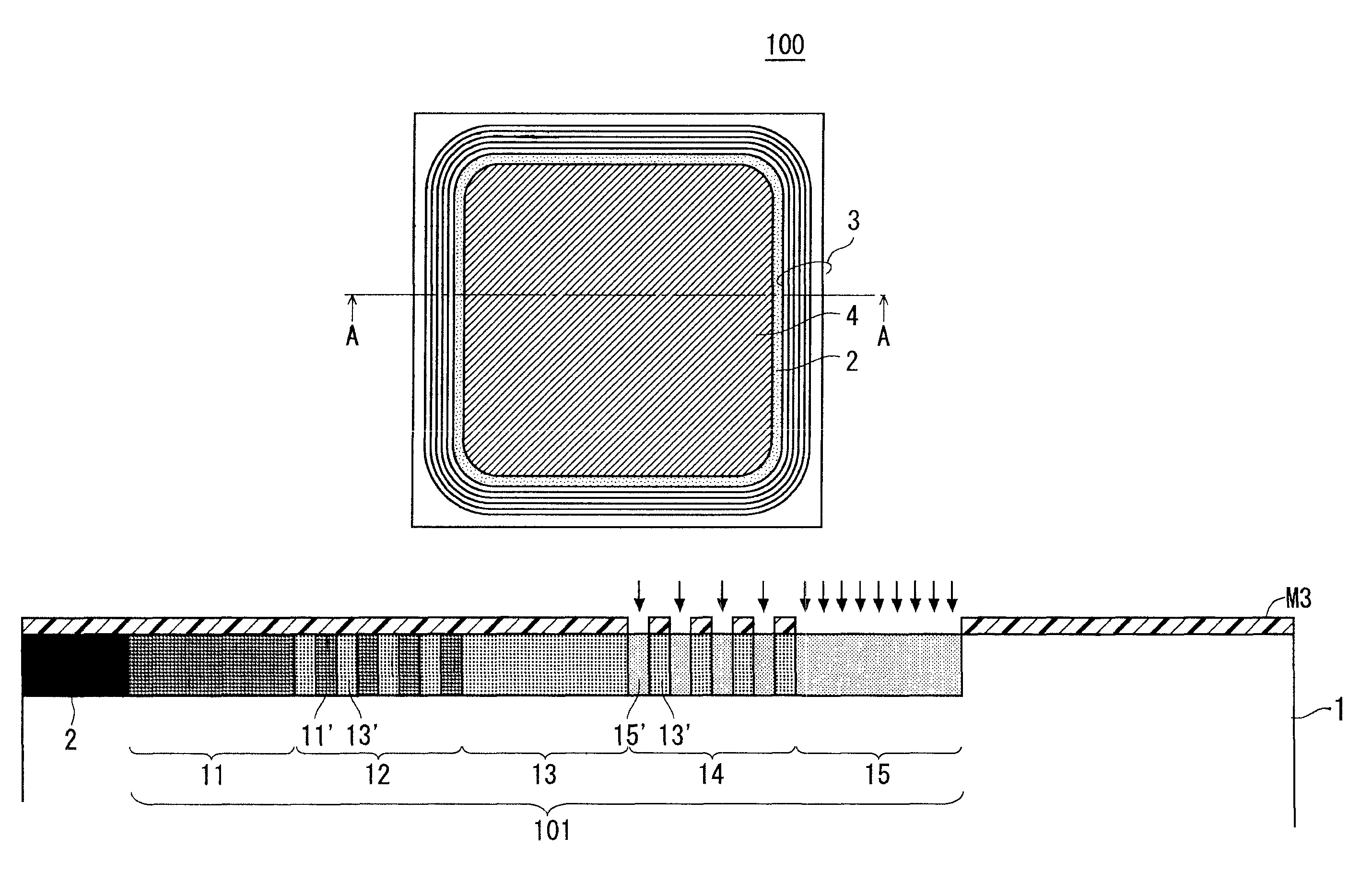
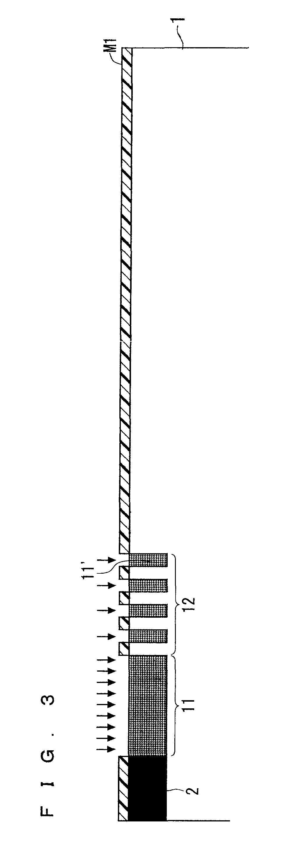
[0061]FIGS. 3 to 5 are cross-sectional views sequentially showing a process of manufacturing the termination region. A final configuration of the termination region is indicated as a RESURF layer 101 in FIG. 5 showing the final step.

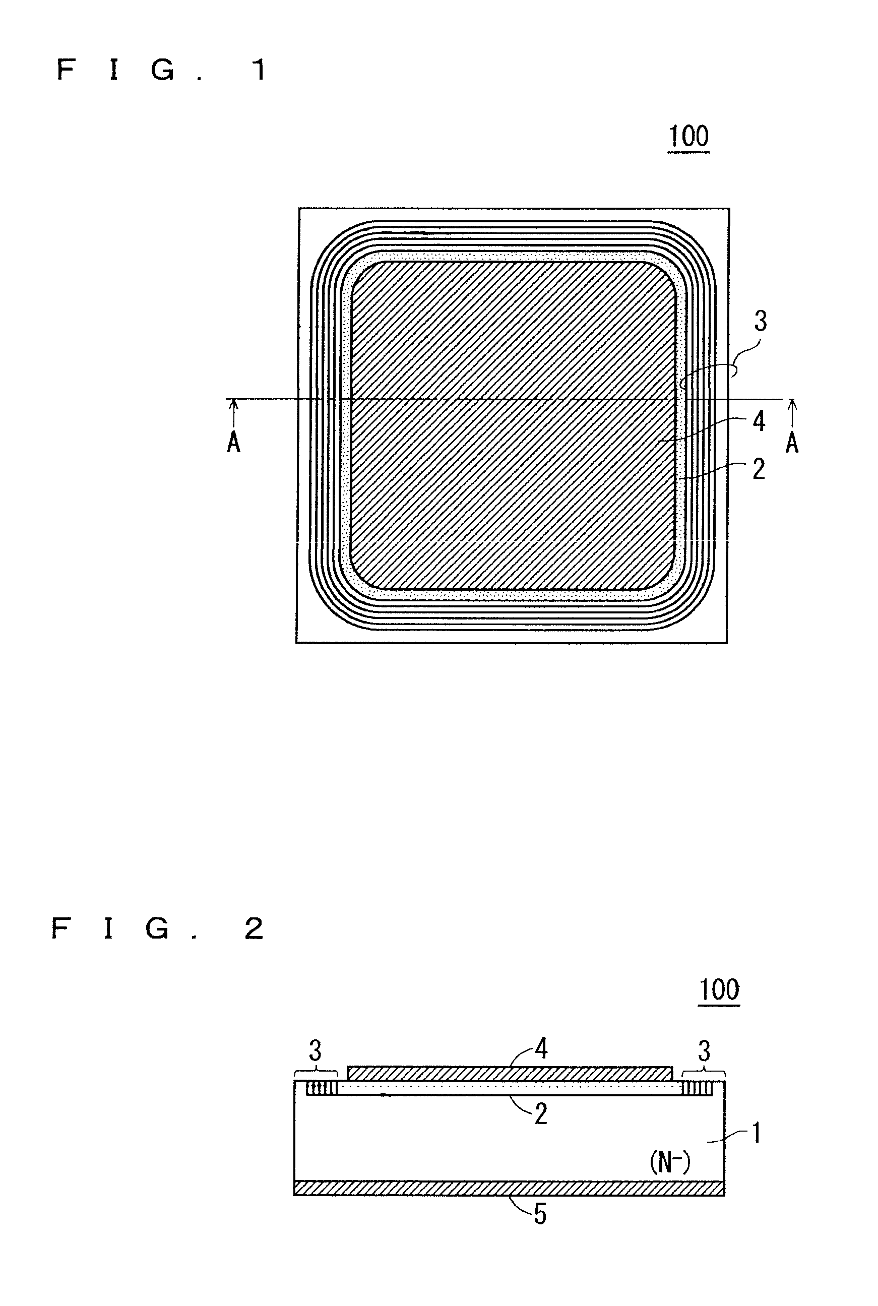
[0062]As shown in FIG. 5, the RESURF layer 101, which includes a plurality of P-type implantation layers containing relatively low concentrations of P-type impurity, is formed adjacent to the active region (P-type base) 2 containing a relatively high concentration of P-type impurity. A region where the RESURF layer 101 is formed serves as the termination region.

[0063]The RESURF layer 101 includes a first RESURF layer 11, a second RESURF layer 12, a third RESURF layer 13, a fourth RESURF layer 14, and a fifth RESURF layer 15 that are ...

embodiment 2

B. Embodiment 2

[0109]A configuration of a method for manufacturing the termination region according to an embodiment 2 of the present invention will be described with reference to FIGS. 12 and 13.

B-1. Device Configuration

[0110]FIGS. 12 and 13 are cross-sectional views sequentially showing a process of manufacturing the termination region. A final configuration of the termination region is indicated as a RESURF layer 101 in FIG. 13 showing the final step. In this embodiment, the configuration of the RESURF layer finally obtained is the same as the configuration of the RESURF layer 101 shown in FIG. 5 according to the embodiment 1, but a method for manufacturing the RESURF layer is different from that of the embodiment 1.

B-2. Manufacturing Method

[0111]In the following, a method for forming the RESURF layer 101 will be described with reference to FIGS. 12 and 13. Firstly, as shown in FIG. 12, an implantation mask M21 is patterned on the main surface where the active region 2 is formed....

modification 3

B-5. Modification 3

[0154]In a case of the diode 100 in which the active region is constituted only by the P-type base 2 as shown in FIG. 1, the implantation of the RESURF layer may be performed over the entire P-type base 2. This method will be described with reference to FIGS. 20 and 21.

[0155]FIGS. 20 and 21 are cross-sectional views sequentially showing a process of manufacturing the termination region. A final configuration of the termination region is indicated as a RESURF layer 102C in FIG. 21 showing the final step.

[0156]The RESURF layer 102C includes an active region RESURF layer 10 extending over the entire P-type base 2, a first RESURF layer 11C, a second RESURF layer 12C, a third RESURF layer 13C, a fourth RESURF layer 14C, a fifth RESURF layer 15C, and a sixth RESURF layer 16C that are arranged in the mentioned order from the P-type base 2 side and arranged so as to surround the P-type base 2.

[0157]The first RESURF layer 11C is configured such that an impurity layer 111 i...


PUM


Abstract

A RESURF layer including a plurality of P-type implantation layers having a low concentration of P-type impurity is formed adjacent to an active region. The RESURF layer includes a first RESURF layer, a second RESURF layer, a third RESURF layer, a fourth RESURF layer, and a fifth RESURF layer that are arranged sequentially from the P-type base side so as to surround the P-type base. The second RESURF layer is configured with small regions having an implantation amount equal to that of the first RESURF layer and small regions having an implantation amount equal to that of the third RESURF layer being alternately arranged in multiple. The fourth RESURF layer is configured with small regions having an implantation amount equal to that of the third RESURF layer and small regions having an implantation amount equal to that of the fifth RESURF layer being alternately arranged in multiple.

Description

TECHNICAL FIELD[0001]The present invention relates to a semiconductor device, and mainly relates to a power semiconductor device having a breakdown voltage of one kilovolt or higher.BACKGROUND ART[0002]In a semiconductor device, as typified by a diode, a MOSFET (Metal-Oxide-Semiconductor Field-Effect-Transistor), and an IGBT (Insulated Gate Bipolar Transistor), a termination region for enhancing breakdown voltage performance is formed so as to surround a region (active region) that functions as an active element.[0003]The breakdown voltage of a semiconductor device includes a reverse breakdown voltage of a diode and an off breakdown voltage of a transistor. Either of them is a breakdown voltage in a case where the semiconductor device does not function as the active element, and a depletion layer spreading in the semiconductor maintains the breakdown voltage performance.[0004]Here, in a semiconductor device having no termination region provided in an active region, only a low breakd...

Claims


Application Information

Patent Timeline
Patent Type & Authority Patents(United States)
IPC IPC(8): H01L29/12
CPCH01L29/66068H01L29/7835H01L29/6606H01L21/266H01L29/063H01L29/0692H01L29/0878H01L29/0634H01L29/1608H01L29/66128H01L29/66143H01L21/0465H01L29/66659H01L29/872H01L29/8611H01L21/265H01L29/12H01L29/0615H01L29/0619
Inventor KAWAKAMI, TSUYOSHIFURUKAWA, AKIHIKOMIURA, NARUHISAKAGAWA, YASUHIROHAMADA, KENJINAKAKI, YOSHIYUKI
Owner MITSUBISHI ELECTRIC CORP
Why Eureka
Try Eureka