Field-effect transistor, and memory and semiconductor circuit including the same

a field-effect transistor and transistor technology, applied in the direction of transistors, solid-state devices, capacitors, etc., can solve the problem of extremely small off-state current that cannot be obtained, and achieve the effect of reducing off-state curren

Inactive Publication Date: 2014-06-17
SEMICON ENERGY LAB CO LTD
View PDF143 Cites 29 Cited by
  • Summary
  • Abstract
  • Description
  • Claims
  • Application Information

AI Technical Summary

Benefits of technology

[0014]With the depletion region 206a, current can be prevented from flowing between the source 204a and the drain 205a; as a result, extremely small off-state current can be obtained. The thinner a gate insulating film 202a becomes and the higher a permittivity thereof becomes, the more effectively electrons can be removed. In addition, the higher the work function of the gate 203a becomes, the more effectively electrons can be removed.
[0017]In an FET including silicon, an increase in off-state current and a degradation of the subthreshold characteristics due to short channel length are known as short channel effects. In an FET including an oxide semiconductor, such short channel effects become more severe. This is because it is hard to form a PN junction in an FET including an oxide semiconductor for dividing a channel formation region from a source or a drain, while a source and a channel formation region, or a drain and a channel formation region can be divided by a PN junction in an FET including silicon.
[0018]In general, for example, in the case where a source and a drain in an FET including silicon are high-concentration N-type regions, a channel formation region is a P-type region having an appropriate concentration. With a PN junction formed in this manner, electrons can be prevented from being injected to a channel from the source or the drain. When the concentration of the P-type impurity in the channel formation region is high, injection of electrons is more effectively prevented. Therefore, in the FET including silicon, when the channel length is short, a short channel effect can be suppressed by an increase of the impurity concentration of the channel formation region.
[0020]In order to achieve miniaturization, it is necessary to shorten the channel length, and it is desired to obtain sufficiently small off-state current even with a short channel. An object of an embodiment of the present invention is to provide an FET in which an increase of off-state current due to a short channel can be prevented. Further, an object of an embodiment of the present invention is to provide a sufficiently miniaturized FET. Furthermore, an object of an embodiment of the present invention is to provide a semiconductor device including an FET. Moreover, an object of an embodiment of the present invention is to provide a method for manufacturing an FET or a semiconductor device. The present invention achieves at least one of the above objects.
[0024]For example, in the case where an In—Zn-based oxide is used, the oxide semiconductor can be formed using an oxide target containing indium (In) and zinc (Zn) at In / Zn=0.5 to 50, preferably In / Zn=1 to 20, more preferably In / Zn=1.5 to 15. Note that in a target used for formation of an In—Zn-based oxide which has an atomic ratio of In:Zn:O=x:y:z, the relation z>1.5x+y is preferably satisfied. When the proportion of indium is increased, the mobility of an FET can be increased.
[0034]In any of the above structures, three surfaces of the thin oxide semiconductor are covered with the gate. Accordingly, electrons injected to the thin oxide semiconductor from the source or the drain can be effectively removed, and most of the region between the source and the drain can be a depletion region, resulting in a reduction in off-state current.

Problems solved by technology

However, the present inventors have found that such extremely small off-state current can be obtained when the channel length is long enough and that because of a short channel effect, the extremely small off-state current cannot be obtained when the channel length is shorter than or equal to 100 nm.

Method used


Image

  • Field-effect transistor, and memory and semiconductor circuit including the same
  • Field-effect transistor, and memory and semiconductor circuit including the same
  • Field-effect transistor, and memory and semiconductor circuit including the same

Examples


embodiment 1

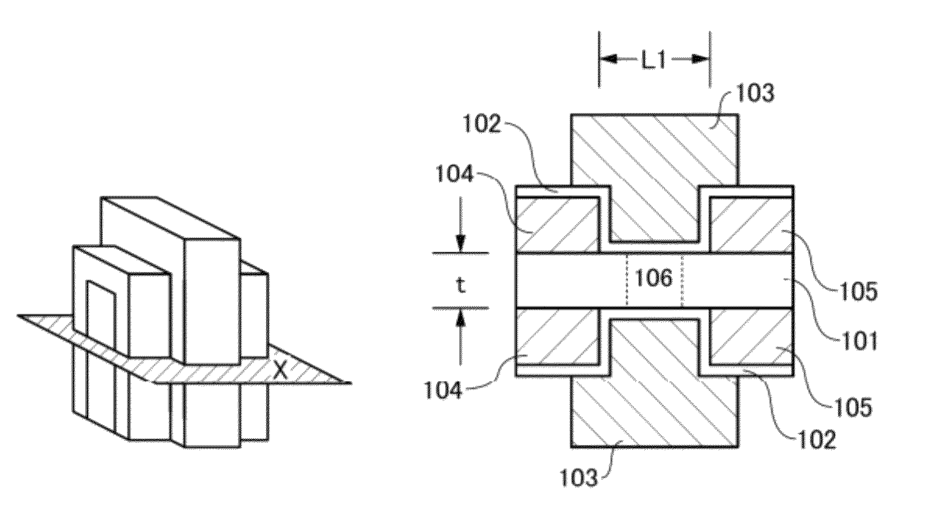
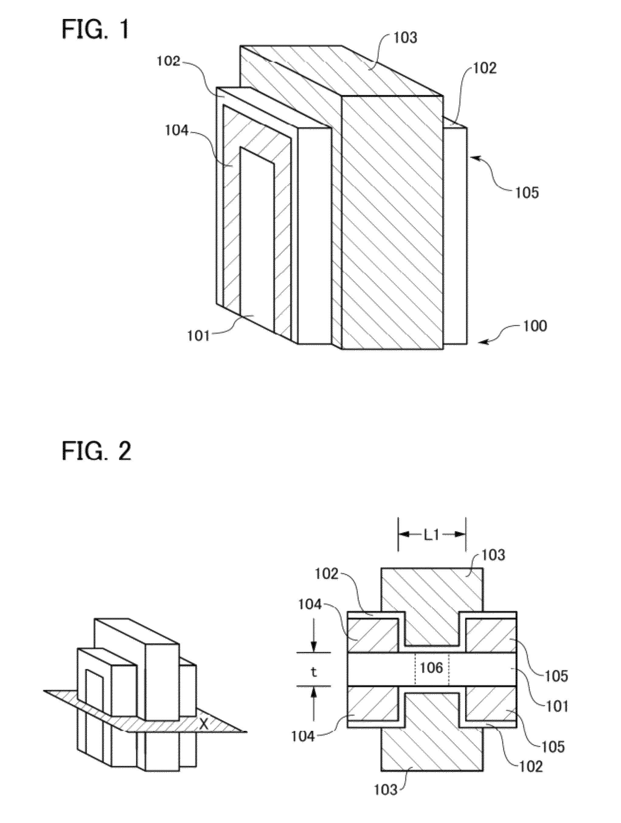
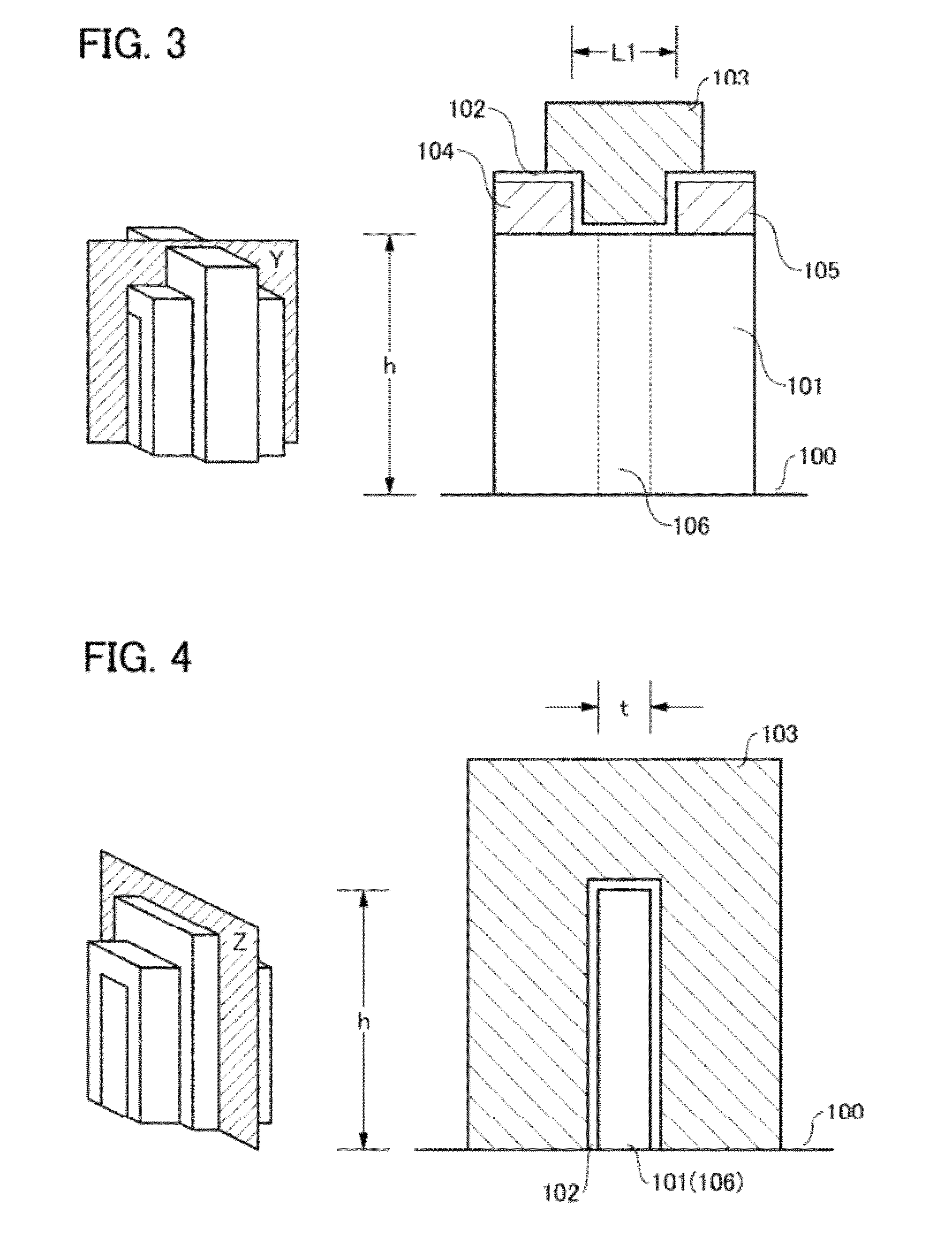
[0052]FIG. 1, FIG. 2, FIG. 3, and FIG. 4 are conceptual views of shapes of an FET of this embodiment. FIG. 1 is a perspective view of the FET. FIG. 2 is a cross-sectional view of the FET cut by a plane X. FIG. 3 is a cross-sectional view of the FET cut by a plane Y. FIG. 4 is a cross-sectional view of the FET cut by a plane Z. The FET illustrated in FIG. 1, FIG. 2, FIG. 3, and FIG. 4 includes a thin oxide semiconductor 101 in contact with an insulating surface 100. A thickness t of the oxide semiconductor 101 is greater than or equal to 1 nm and less than or equal to 30 nm, preferably greater than or equal to 3 nm and less than or equal to 5 nm, and a height h of the oxide semiconductor 101 is greater than or equal to 5 nm and less than or equal to 100 nm, preferably greater than or equal to 10 nm and less than or equal to 50 nm.

[0053]The oxide semiconductor 101 preferably has a crystal structure, and preferably includes CAAC-OS described above. In this case, the oxide semiconductor...

embodiment 2

[0062]FIGS. 5A and 5B illustrate an FET of this embodiment. FIG. 5A is a cross-sectional view of the FET cut by a plane X, which corresponds to FIG. 2. FIG. 5B is a cross-sectional view of the FET cut by a plane Y, which corresponds to FIG. 3. Note that a cross-sectional view of the FET of this embodiment cut by a plane Z is the same as FIG. 4.

[0063]The FET of this embodiment includes the oxide semiconductor 101 which is in contact with the insulating surface 100. The source 104 and the drain 105 are provided in contact with part of the oxide semiconductor 101. Further, the FET includes the gate insulating film 102 which covers the oxide semiconductor 101, the source 104, and the drain 105 and is provided in contact with the oxide semiconductor 101. Furthermore, the gate 103 is provided to cover the gate insulating film 102. The FET of this embodiment is different from the FET of Embodiment 1 in that the gate 103 is provided so as not to overlap with either the source 104 or the dra...

embodiment 3

[0075]FIGS. 6A and 6B illustrate an FET of this embodiment. FIG. 6A is a cross-sectional view of the FET cut by a plane X, which corresponds to FIG. 2. FIG. 6B is a cross-sectional view of the FET cut by a plane Y, which corresponds to FIG. 3. Note that a cross-sectional view of the FET of this embodiment cut by a plane Z is the same as FIG. 4. The FET of this embodiment includes the oxide semiconductor 101 in contact with the insulating surface 100.

[0076]The source 104 and the drain 105 are provided in contact with part of the oxide semiconductor 101. The FET includes the gate insulating film 102 which covers the oxide semiconductor 101, the source 104, and the drain 105 and is provided in contact with the oxide semiconductor 101. Further, the gate 103 is formed to cover the gate insulating film 102. The gate 103 is provided so as not to overlap with either the source 104 or the drain 105, which is similar to the FET of Embodiment 2.

[0077]The FET of this embodiment is different fro...


PUM


Abstract

Provided is a field-effect transistor (FET) having small off-state current, which is used in a miniaturized semiconductor integrated circuit. The field-effect transistor includes a thin oxide semiconductor which is formed substantially perpendicular to an insulating surface and has a thickness of greater than or equal to 1 nm and less than or equal to 30 nm, a gate insulating film formed to cover the oxide semiconductor, and a strip-like gate which is formed to cover the gate insulating film and has a width of greater than or equal to 10 nm and less than or equal to 100 nm. In this structure, three surfaces of the thin oxide semiconductor are covered with the gate, so that electrons injected from a source or a drain can be effectively removed, and most of the space between the source and the drain can be a depletion region; thus, off-state current can be reduced.

Description

BACKGROUND OF THE INVENTION[0001]1. Field of the Invention[0002]The present invention relates to a field-effect transistor and a semiconductor device including it.[0003]2. Description of the Related Art[0004]A field-effect transistor (hereinafter, FET) used for a semiconductor integrated circuit or the like has been conventionally formed using a semiconductor such as silicon (see Non-Patent Document 1, for example). In recent years, a field-effect transistor including an oxide semiconductor having a band gap of 2.5 eV or more is reported. In particular, it has been revealed that by extremely lowering the donor concentration in a semiconductor layer, off-state current can be lowered to a value which cannot be measured by an ordinal method (see Patent Document 1, for example).[0005]For example, the off-state current per micrometer of the channel width is generally larger than or equal to 1×10⁻¹⁵ A / μm in an FET including silicon, while the off-state current per micrometer of the channe...

Claims


Application Information

Patent Timeline
Patent Type & Authority Patents(United States)
IPC IPC(8): H01L29/12
CPCH01L27/0688H01L27/108H01L27/1225H01L27/10826H01L28/90H01L27/1156H01L27/10894H01L29/785H01L27/10897H01L29/41733H01L27/1203H01L29/78609H01L29/7869H01L27/10879H01L27/10805H01L27/10852H10B12/36H10B12/056H10B12/00H10B12/09H10B12/50H10B12/033H10B41/70H01L29/78696H10B12/30
Inventor YAMAZAKI, SHUNPEIGODO, HIROMICHITAKEMURA, YASUHIKO
Owner SEMICON ENERGY LAB CO LTD
Why Eureka
Try Eureka