Surface emitting laser diode, optical scanning apparatus and image forming apparatus

a laser diode and laser array technology, applied in semiconductor lasers, instruments, electrographic processes, etc., can solve the problem of difficult manufacturing of surface emitting laser diodes having single transverse, and achieve the effect of high yield ra

Inactive Publication Date: 2014-07-08
RICOH KK
View PDF38 Cites 2 Cited by
  • Summary
  • Abstract
  • Description
  • Claims
  • Application Information

AI Technical Summary

Benefits of technology

[0016]According to the devices and methodologies of this disclosure, high single transverse mode, stabilized polarization direction, isotropic beam cross section and small divergence angle may be realized in high yield rate.

Problems solved by technology

However, even if the conventional technologies are combined, it is difficult to manufacture surface emitting laser diode having single transverse mode, high power, stable polarization direction, isotropic cross sectional shape of output beam and small divergence angle with high productivity.

Method used


Image

  • Surface emitting laser diode, optical scanning apparatus and image forming apparatus
  • Surface emitting laser diode, optical scanning apparatus and image forming apparatus
  • Surface emitting laser diode, optical scanning apparatus and image forming apparatus

Examples


first modified embodiment

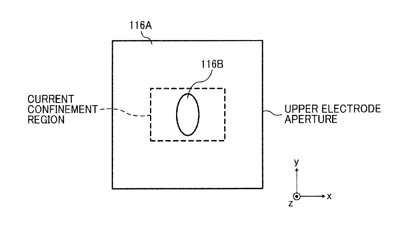
[0191]FIG. 37 shows first modified embodiment of surface emitting laser diode array. The upper semiconductor DBR 107 includes a low refractive index layer 107b existing in +z axis direction made of p-Al0.9Ga0.1As. A semiconductor layer 118 having larger refractive index than the low refractive index layer 107b is formed with an optical thickness of λ / 4 in +z axis direction. Further, the part of semiconductor layer 118 included in the emission region is removed by etching process. The part which the semiconductor layer 118 is removed corresponds to the semiconductor surface structure 116A and the center part which the semiconductor layer 118 is not removed corresponds to the semiconductor surface structure 116B.

[0192]In the first modified embodiment, the same effects may be realized as same as the surface emitting laser diode array 100.

second modified embodiment

[0193]FIG. 38 shows second modified embodiment of surface emitting laser diode array. In this embodiment, the emission region of the surface emitting laser diode array of the first modified embodiment is covered by a dielectric layer 119 having an optical thickness of 2λ / 4. For example, the layer 119 occupies the aperture in the upper electrode 113.

[0194]In the second modified embodiment, additionally, oxidation and pollution of the emission region may be prevented.

[0195]The dielectric layer 118 may be made of any one of SiN, SiO2, SiON, ZrO2, TiO2 and TiN. The dielectric layer 118 may be formed by plasma CVD, electron beam deposition, physical vapor deposition and relative sputtering.

[0196]The optical thickness of the dielectric layer 119 becomes even multiple of λ / 4.

third modified embodiment

[0197]FIG. 39 shows second modified embodiment of surface emitting laser diode array. In this embodiment, the emission region of the surface emitting laser diode array 100 is covered by a low refractive dielectric layer 120 having an optical thickness of λ / 4 and a high refractive dielectric layer 121 having an optical thickness of λ / 4.

[0198]In the third modified embodiment, additionally, reliability and durability may be improved.

[0199]The optical thickness of each dielectric layer becomes odd multiple of λ / 4. The pair of the dielectric layer 120 and the dielectric layer 121 may be multiple.

[0200]According to the surface emitting laser diode array 100 of the present embodiment, each emitting part includes the buffer layer 102, the lower semiconductor DBR 103, the resonator structure including the active layer, the upper semiconductor DBR 107 on the substrate 101. The upper electrode 113 surrounds the emission region which outputs laser beam.

[0201]The emission region includes the sem...


PUM


Abstract

A surface emitting laser diode comprises a substrate, a lower reflector formed over the substrate, an active layer formed over the lower reflector, an upper reflector formed over the active layer, a current restrict structure including a current confinement region surrounded by insulation region. The current restrict structure is disposed in an upper reflector or between an active layer and the upper reflector, and an upper electrode formed over the upper reflector includes an aperture which corresponds to an emission region from which light is emitted in a first direction perpendicular to a surface of a substrate. The emission region and the current restrict structure including the current confinement region are selectively configured to obtain high single transverse mode, stabilized polarization direction, isotropic beam cross section and small divergence angle, while allowing the device to be manufactured with high yield rate.

Description

CROSS-REFERENCE TO RELATED APPLICATIONS[0001]The present application claims priority to, and incorporates by reference the entire contents of, Japanese Patent Application No. 2011-110127 filed with the Japanese Patent Office on May 17, 2011 and Japanese Patent Application No. 2012-020444 filed with the Japanese Patent Office on Feb. 2, 2012BACKGROUND[0002]1. Technical Field[0003]This disclosure generally relates to surface emitting laser diode, surface emitting laser array, optical scanning device and image forming apparatus, and more particularly to a surface emitting laser diode emitting a laser beam in a direction perpendicular to a substrate, a surface emitting laser array including a plurality of such surface emitting laser diodes, an optical scanning device having such a surface emitting laser array, and an image forming apparatus having such an optical scanning device.[0004]2. Description of the Related Art[0005]A surface emission laser diode of vertical cavity surface emissi...

Claims


Application Information

Patent Timeline
Patent Type & Authority Patents(United States)
IPC IPC(8): H01S5/00
CPCH01S5/3403B82Y20/00G03G15/04072H01S5/0421H01S5/18355H01S5/0014H01S5/18313H01S5/423H01S5/18338H01S5/0655H01S5/18333H01S5/3202H01S5/18394H01S2301/185G02B26/123H01S5/3436
Inventor ITOH, AKIHIROHARASAKA, KAZUHIROSATO, SHUNICHIJIKUTANI, NAOTO
Owner RICOH KK
Why Eureka
Try Eureka