
Amber light-emitting diode comprising a group III-nitride nanowire active region

a light-emitting diode and amber technology, applied in the field of temperature stable amber light-emitting diodes, can solve the problems of significant stokes loss, decreased led efficiency, and inability to achieve significant stokes loss, high indium content, and high material quality

Active Publication Date: 2014-07-22
NAT TECH & ENG SOLUTIONS OF SANDIA LLC
View PDF6 Cites 22 Cited by
  • Summary
  • Abstract
  • Description
  • Claims
  • Application Information

AI Technical Summary

Benefits of technology

This patent describes a new way to make LEDs that produce amber light. Using a special structure made of nanowires and planar layers, researchers have been able to create more efficient and stable LEDs compared to previous methods. These LEDs have higher concentrations of indium, which helps them produce yellow, orange, and potentially red light with great efficiency. This new technology can be used to create high-efficiency white LEDs using a specific color-mixing approach.

Problems solved by technology

Although additional phosphors can be added to broaden the emitted spectrum and improve the Color Rendering Index (CRI) and reach warmer color temperatures, it is at a cost to device efficacy.
While pc-LEDs currently represent the most popular approach for high intensity white LEDs, they suffer from certain disadvantages, most notably Stokes losses, which are an unavoidable consequence of the energy down-conversion process and result in decreases in LED efficiency.
While improvements in phosphor efficiencies continue to be made, significant Stokes losses are inevitable.
However, while high efficiency LEDs exist in the blue wavelengths, realization of high efficiency discrete color mixed RYGB LEDs is seriously hindered by a lack of efficient and temperature stable LEDs in the yellow-red wavelengths (and to a lesser extent in the green).
This long wavelength gap is a consequence of the difficulties in forming high quality InGaN films with the higher indium concentrations needed to achieve the longer wavelengths (lower bandgaps) due to lattice mismatch strain effects with GaN.
Red LEDs based on the AlInGaP materials system, while efficient at longer red wavelengths, are much less efficient at the shorter red (615 nm) and amber (580-590 nm) wavelengths needed for high efficiency and high CRI color-mixed white LEDs due to limitations in that material system.
The limitations of poor carrier confinement and carrier losses to indirect parts to the AlInGaP bandstructure are fundamental, and most likely impossible to overcome.
Moreover, these limitations of red and yellow AlInGaP LEDs also lead to poor temperature stability and additional efficiency losses and color shifts at operating temperatures typical of high brightness LEDs (e.g. 125° C.).
While currently competitive, pc-LEDs are unable to meet the targets of 81% EQE for green, red, and amber LEDs, which will likely require more efficient direct-emitting LEDs.
Current direct-emitting red and amber LEDs based on the AlInGaP materials system suffer from significant efficiency losses and color shifts at the higher operating temperatures typical of high brightness LEDs.

Method used


Image

  • Amber light-emitting diode comprising a group III-nitride nanowire active region
  • Amber light-emitting diode comprising a group III-nitride nanowire active region
  • Amber light-emitting diode comprising a group III-nitride nanowire active region

Examples


Embodiment Construction

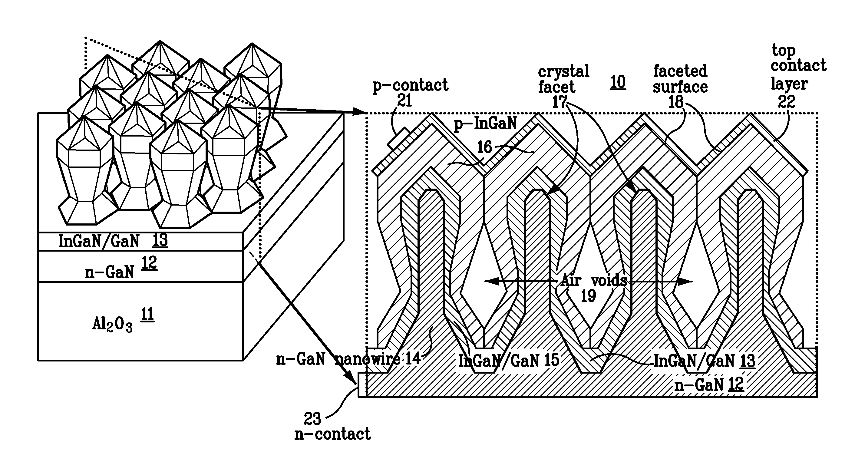
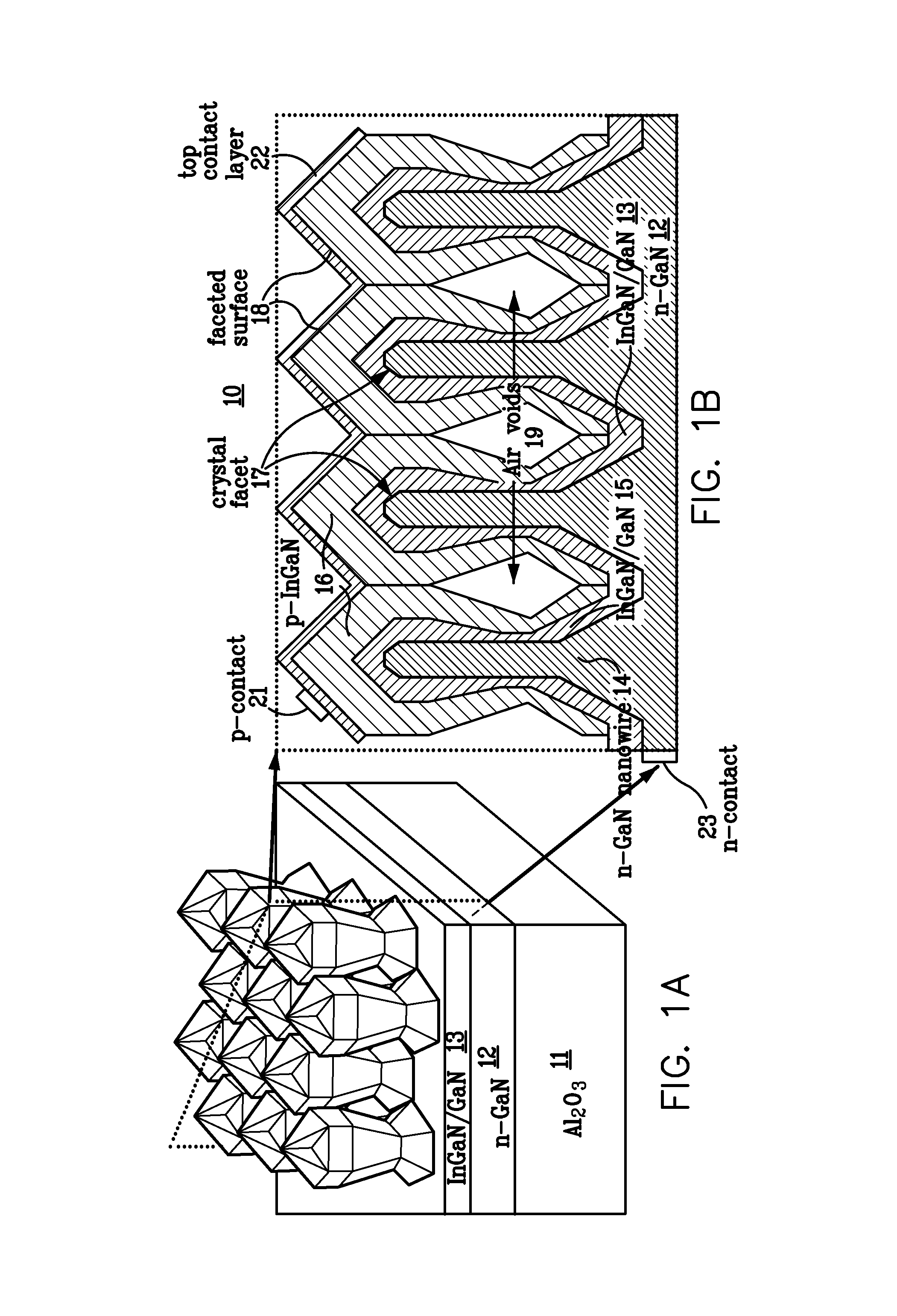
[0016]According to the present invention, amber LEDs (˜585 nm) with high efficiencies and high temperature stability based on the InGaN materials system can be fabricated by employing a novel three-dimensional, hybrid core-shell device structure. In this structure, the active emitter MQW regions are grown on a high quality nanowire template, while a top coalesced p-type (In)GaN layer enables standard planar device processing. The nanowire architecture allows for growth of higher indium content InGaN layers than is possible in standard planar InGaN / GaN film heterostructures, due to the unique ability of nanowires to accommodate lattice mismatch strain owing to their large free surface area and nanoscale dimensions. See T. Kuykendall et al., Nature Mater. 6, 951 (2007); and Q. M. Li and G. T. Wang, Appl. Phys. Lett. 97, 181107 (2010). While indium concentrations greater than ˜20% in planar InGaN on GaN material lead to a significant degradation in the material and hence optical qualit...


PUM

PropertyMeasurementUnit
wavelengthaaaaaaaaaa
heightaaaaaaaaaa

Abstract

A temperature stable (color and efficiency) III-nitride based amber (585 nm) light-emitting diode is based on a novel hybrid nanowire-planar structure. The arrays of GaN nanowires enable radial InGaN / GaN quantum well LED structures with high indium content and high material quality. The high efficiency and temperature stable direct yellow and red phosphor-free emitters enable high efficiency white LEDs based on the RGYB color-mixing approach.

Description

CROSS-REFERENCE TO RELATED APPLICATIONS[0001]This application claims the benefit of U.S. Provisional Application No. 61 / 588,446, filed Jan. 19, 2012, which is incorporated herein by reference. This application is related to U.S. application Ser. No. 13 / 434,646, filed Mar. 29, 2012, and SD11787.1, “Method of Fabricating Vertically Aligned Group III-V Nanowires,” filed of even date with this application, both of which are incorporated herein by reference.STATEMENT OF GOVERNMENT INTEREST[0002]This invention was made with Government support under contract no. DE-AC04-94AL85000 awarded by the U.S. Department of Energy to Sandia Corporation. The Government has certain rights in the invention.FIELD OF THE INVENTION[0003]The present invention relates to light-emitting diodes and, in particular, to a temperature stable amber light-emitting diode (LED) that employs a Group III-Nitride nanowire active region.BACKGROUND OF THE INVENTION[0004]Two common approaches currently exist for producing w...

Claims


Application Information

Patent Timeline
Patent Type & Authority Patents(United States)
IPC IPC(8): H01L29/06H01L29/15B82Y40/00H01L33/04
CPCB82Y40/00H01L33/04H01L33/18H01L33/24Y10S977/762B82Y30/00
Inventor WANG, GEORGE T.LI, QIMINGWIERER, JR., JONATHAN J.KOLESKE, DANIEL
Owner NAT TECH & ENG SOLUTIONS OF SANDIA LLC
Learn More