Method for forming Si-containing film using two precursors by ALD

a technology of atomic layer and precursor, applied in the direction of coating, chemical vapor deposition coating, metallic material coating process, etc., can solve the problems of difficult deposition of sin film, low throughput of film forming process, and inability to easily chemisorbed precursors on the surface of substrates, etc., to achieve the effect of improving the growth rate per cycl

Active Publication Date: 2014-12-16
ASM IP HLDG BV
View PDF8 Cites 380 Cited by
  • Summary
  • Abstract
  • Description
  • Claims
  • Application Information

AI Technical Summary

Benefits of technology

[0012]According to the above embodiment, in one cycle of ALD, more than one monolayer can be deposited by using two certain precursors which are reactive with each other without a reactant, thereby improving a growth rate per cycle.

Problems solved by technology

However, because ALD deposits atomic layers one by one by repeating the steps described above, there is a problem of a low throughput of the film forming processes, and when forming a thick film, the steps must be repeated for a high number of times. Further, in ALD, some precursors are not easily chemisorbed on a surface of a substrate.
For example, deposition of SiN film is challenging.
In practice, the only organosilicon precursors feasible for SiN deposition are those containing no oxygen, and therefore, the prime candidates are silicon alkylamides, which are volatile enough to be used in practical applications, but thermal and also plasma-enhanced ALD of SiN from these precursors has not yet been successful.

Method used


Image

  • Method for forming Si-containing film using two precursors by ALD
  • Method for forming Si-containing film using two precursors by ALD
  • Method for forming Si-containing film using two precursors by ALD

Examples


example 1

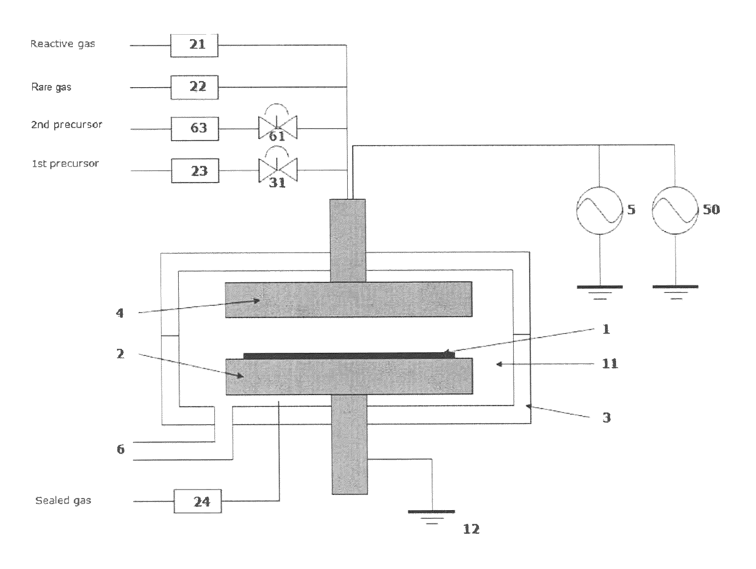
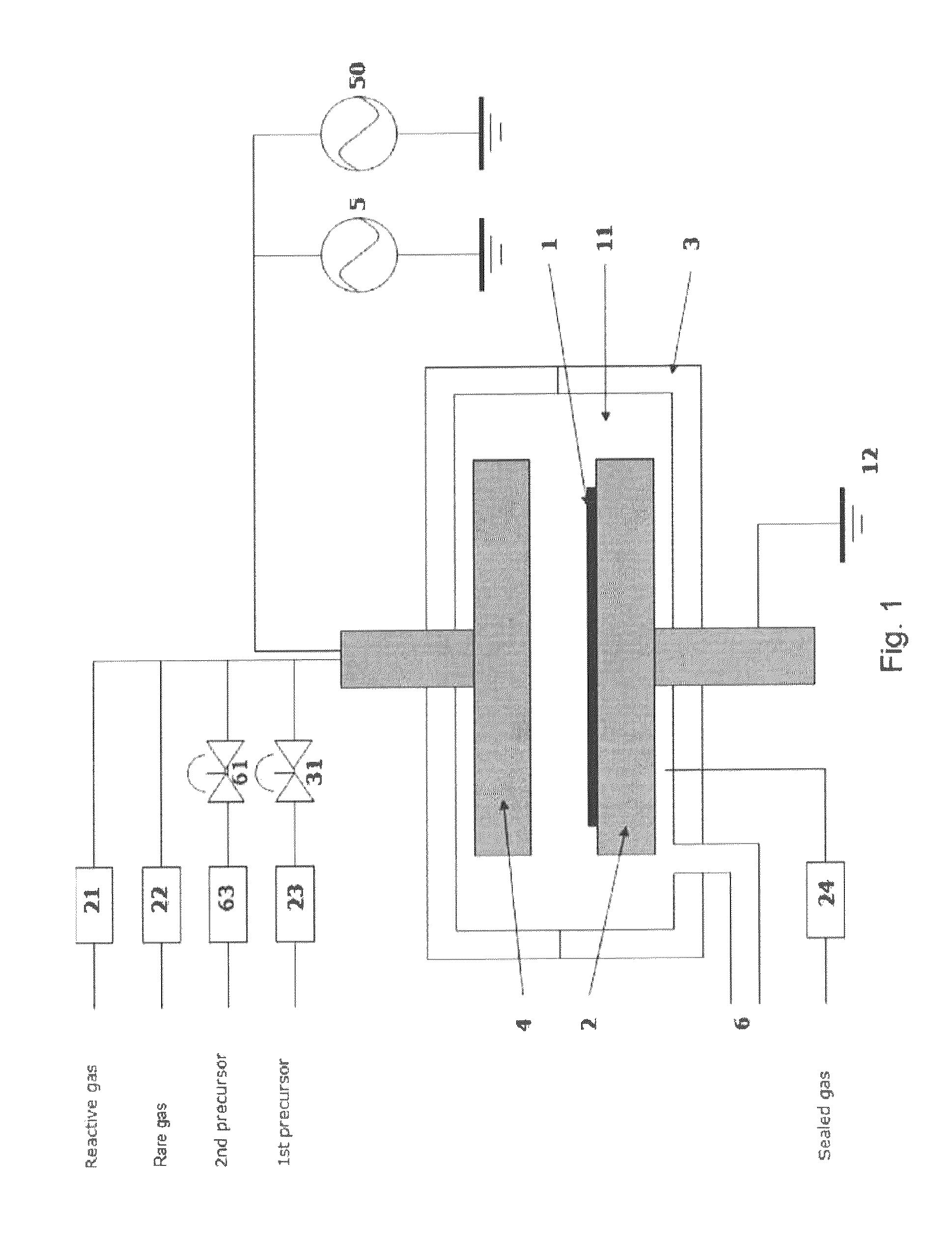
[0044]A dielectric layer having Si—C bonds was formed on a substrate (200 mm in diameter) having a pattern with an opening of 50 nm under the conditions shown below using the sequence illustrated in FIG. 2 and the PEALD apparatus illustrated in FIG. 1.

[0045]Tetrachlorodimethyldisilane (first precursor): 0.1 sccm

[0046]Divinyldimethylsilane (second precursor): 0.4 sccm

[0047]Hydrogen (reactant): 10 sccm

[0048]Helium (reactant): 1000 sccm

[0049]Seal helium: 100 sccm

[0050]Substrate temperature: 100° C.

[0051]High frequency RF power (a frequency of 13.56 MHz): 100 W

[0052]First precursor supply time: 1.0 sec supply

[0053]Second precursor supply time: 1.0 sec supply

[0054]Purge time after each precursor pulse: 3.0 sec

[0055]RF Plasma exciting time: 1.0 sec excite

[0056]Purge time after RE exciting pulse: 1.0 sec

[0057]Number of cycles: 334

[0058]The refractive index, growth rate, etch rate, and step coverage of the deposited film are shown in Table 2.

example 2

[0059]Under conditions which were the same as in Example 1 except the following, a dielectric layer having Si—C bonds was formed on a substrate (200 mm in diameter).

[0060]Substrate temperature: 400° C.

[0061]The refractive index, growth rate, etch rate, and step coverage of the deposited film are shown in Table 2.

example 3

[0062]Under conditions which were the same as in Example 1 except the following, a dielectric layer having Si—C bonds was formed on a substrate (200 mm in diameter).

[0063]CH4 (reactant): 100 sccm

[0064]Hydrogen (reactant): 10 sccm

[0065]Helium (reactant): 1000 sccm

[0066]The refractive index, growth rate, etch rate, and step coverage of the deposited film are shown in Table 2.


PUM

PropertyMeasurementUnit
frequencyaaaaaaaaaa
temperatureaaaaaaaaaa

Abstract

A method for forming a silicon-containing dielectric film on a substrate by atomic layer deposition (ALD) includes: providing two precursors, one precursor containing a halogen in its molecule, another precursor containing a silicon but no halogen in its molecule, adsorbing a first precursor, which is one of the two precursors onto a substrate to deposit a monolayer of the first precursor; adsorbing a second precursor, which is the other of the two precursors onto the monolayer of the first precursor to deposit a monolayer of the second precursor; and exposing the monolayer of the second precursor to radicals of a reactant to cause surface reaction with the radicals to form a compound monolayer of a silicon-containing film.

Description

CROSS-REFERENCE TO RELATED APPLICATIONS[0001]This is an application for patent which claims the benefit of U.S. Provisional Application No. 61 / 611,477, filed Mar. 15, 2012, under 35 USC 119(e), the disclosure of which is herein incorporated by reference in its entirety.BACKGROUND OF THE INVENTION[0002]1. Field of the Invention[0003]The present invention generally relates to atomic layer deposition (ALD) technology, particularly, to a method for depositing a silicon-containing film using two precursors by ALD.[0004]2. Description of the Related Art[0005]Conventionally, in the field of semiconductor manufacturing, a high-quality thin film is deposited on a substrate typically by chemical vapor deposition (CVD). Recently, in connection with development of super fine semiconductor devices, ALD technology, wherein a thin film is formed on a substrate by laminating atomic layers one by one, has been examined. In ALD, a gas-phase source gas is introduced to a chamber wherein a substrate is...

Claims


Application Information

Patent Timeline
Patent Type & Authority Patents(United States)
IPC IPC(8): C23C16/34C23C16/455H01L21/31H01L21/02C23C16/32H01L21/469H01L21/768
CPCH01L21/0217H01L21/02274H01L21/02211H01L21/0228H01L21/02167H01L21/02164C23C16/4554C23C16/325H01L21/76829C23C16/345C23C16/45534
Inventor TSUJI, NAOTOFUKAZAWA, ATSUKITAKAMURE, NOBORUHAUKKA, SUVINISKANEN, ANTTI JUHANIPARK, HYUNG SANG
Owner ASM IP HLDG BV
Why Eureka
Try Eureka