Non-etching non-resist adhesion composition and method of preparing a work piece

a non-etching, non-resist adhesion technology, applied in the direction of resistive material coating, non-metallic protective coating application, textiles and paper, etc., can solve the problems of not being able to accept the risk of completely removing the copper layer in at least one region on the surface, and not being able to use etching solutions in recent most sophisticated processes, etc., to achieve good adhesion of resist coating

Active Publication Date: 2015-02-03
ATOTECH DEUT GMBH
View PDF18 Cites 0 Cited by
  • Summary
  • Abstract
  • Description
  • Claims
  • Application Information

AI Technical Summary

Benefits of technology

[0013]It is therefore an object of the present invention to provide a method to achieve good adherence of a resist coating, more specifically a photo imageable resist coating, to a copper base while ensuring that the copper base being very thin is not compromised by the method.
[0032]Consistency and adherence have been proved excellent. This is in spite of the fact that the copper surface is not substantially affected by the pretreatment method of the invention, i.e., no noticeable roughening takes place when the copper surface is treated in accordance with the invention. Therefore, there is no risk as to excessive removal of copper due to the treatment as with previous methods. Such removal would particularly be important if the copper surface presented is very thin such as in semi-additive processing. Base substrates used in printed circuit board manufacturing for high-sophisticated applications comprise an electroless copper base layer which is only about 1 μm thick and onto which a photo imageable resist is laminated and processed to form a circuitry. As copper pretreatment according to the present invention does virtually not remove any copper from such thin copper base layers, there is, even in portions of the surface area, no risk of complete copper removal. Copper removal using the compounds according to the invention has emerged to be at most 0.1 to 0.2 μm of copper.

Problems solved by technology

The aforementioned etching solutions, however, are not suitable to be used in recent most sophisticated processes in which finest lines and other structures on the printed circuit boards are generated, like 5 μm lines and 5 μm spaces.
For this reason, there will be the risk to totally remove the copper layer in at least part of the region on the surface due to the microetching step.
This of course, will not be acceptable.
For this reason, etching is considered detrimental to the consistency of the copper base.
It has yet been ascertained that benzotriazole is not effective as non-etching adhesion promoter because it can only react with the metal surface and not with the photo imageable resist.

Method used


Image

  • Non-etching non-resist adhesion composition and method of preparing a work piece
  • Non-etching non-resist adhesion composition and method of preparing a work piece
  • Non-etching non-resist adhesion composition and method of preparing a work piece

Examples


example 1

Concentration Dependency

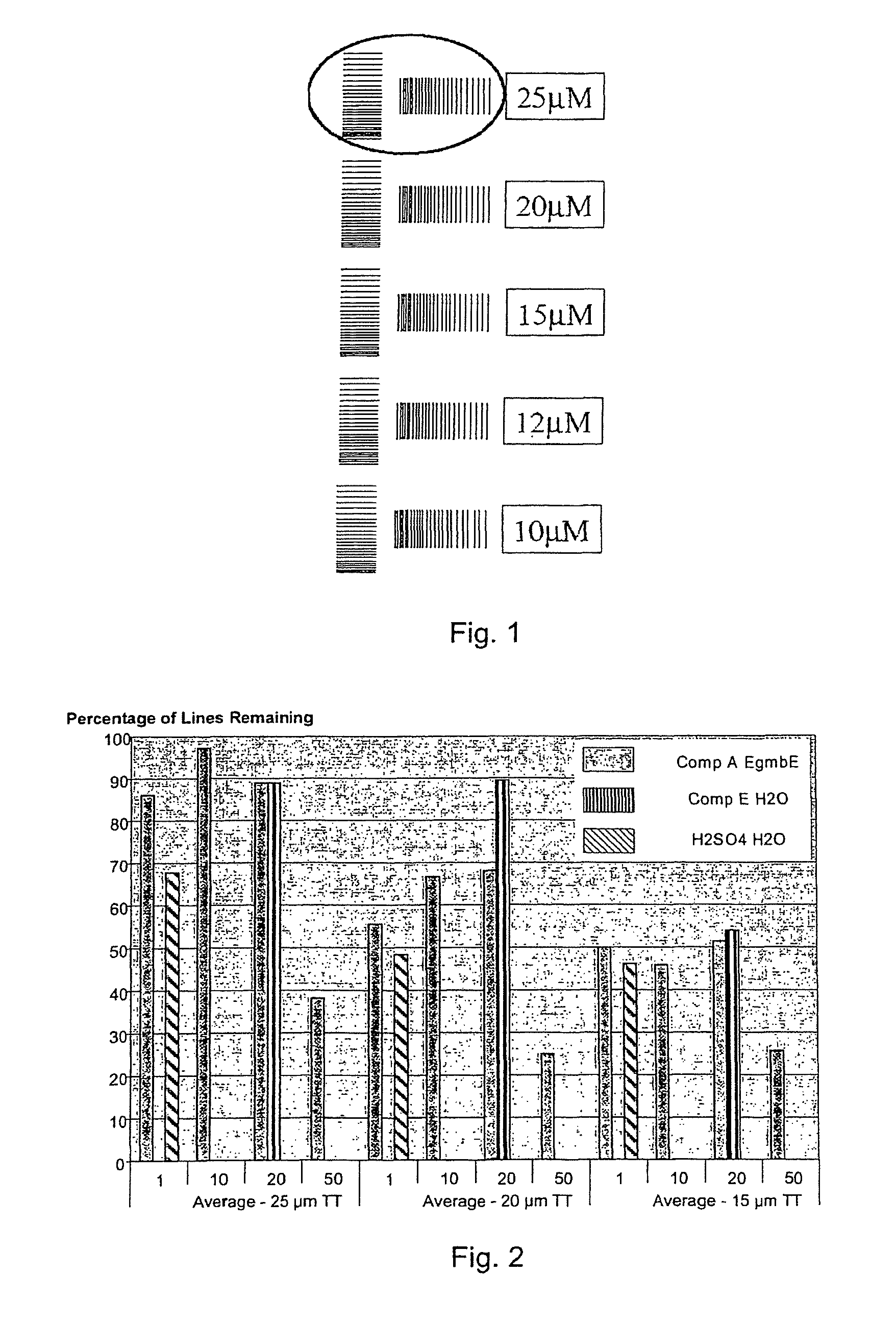
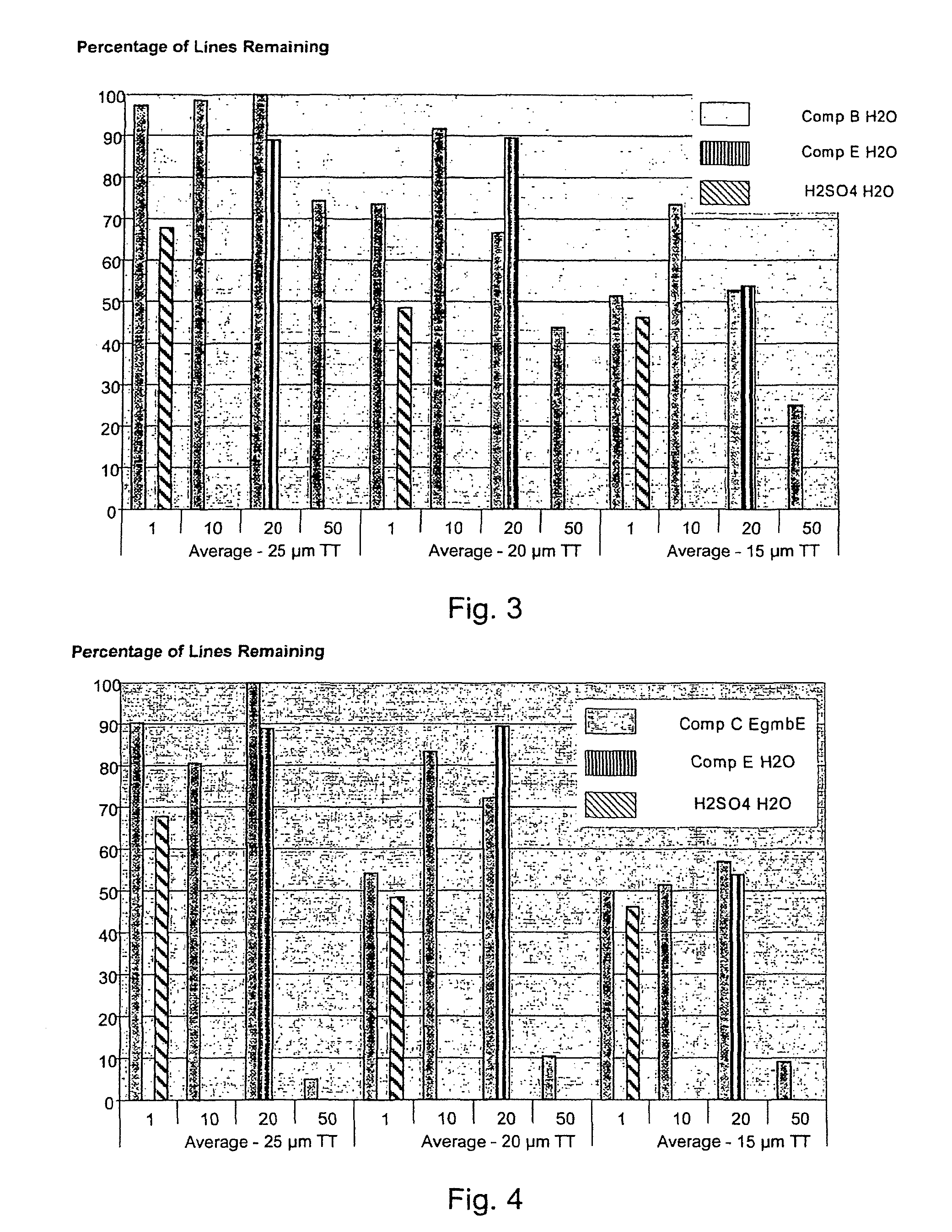
[0139]First tests were performed on test panels Type A. The results obtained with the acrylic compounds A, B, C and D were in each case compared to results obtained with heterocyclic compound E according to the invention and with reference sample X (FIGS. 2-5). As there could not be detected any significant difference between the individual compounds and the reference sample being tested before applying a Scotch® tape, the graphs shown in FIGS. 2-5 refer to line integrity after tape testing.

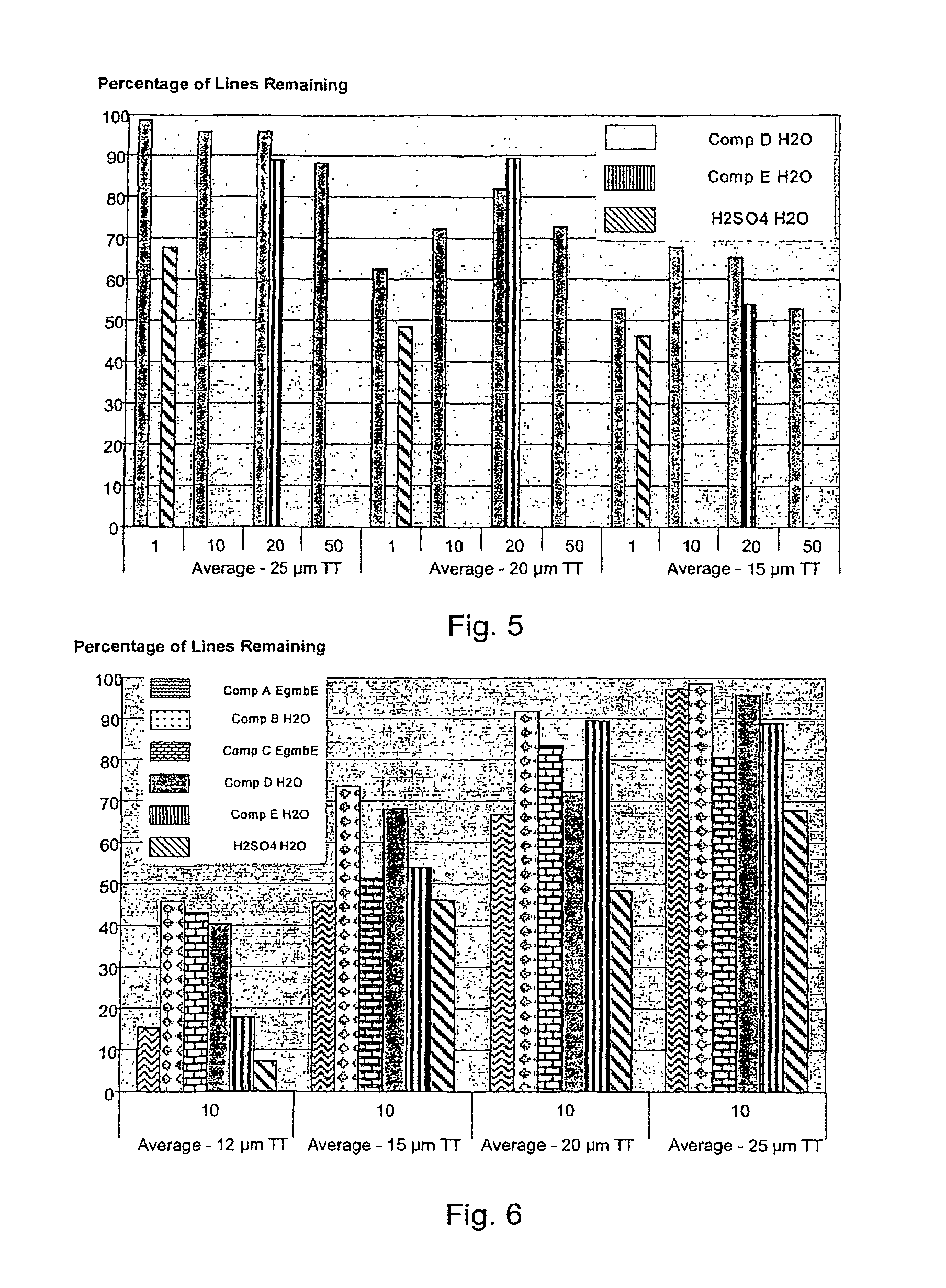
[0140]A concentration of compounds A, B, C, D and E of 10-20 mg / l was found to give best performance. Adhesion performance of all compounds was superior compared to reference sample X. A comparison of the results for 10 mg / l compositions containing the compounds and for the reference sample X is shown in FIG. 6. Interestingly, compounds A and C performed in most cases a little worse than compounds B and D. This difference was believed to be due to the solvent being used to...

example 2

Solvent and Panel Type Influence

[0141]This experiment was performed to observe the effect of the solvent and of the panel type on line integrity. Therefore, all tests were made on test panels Type A and Type B. Furthermore, acrylic compounds C and D were both dissolved in deionized water or in ethylene glycol monobutylether, respectively, in order to directly compare the influence of this solvent. The concentration of these compounds in the adhesion agent composition was 10 mg / l.

[0142]The results obtained after tape testing are shown in FIG. 7 (Type A material) and FIG. 8 (Type B material).

[0143]For Type A material, compound B being dissolved in ethylene glycol monobutylether to give the standard solution, gave similar results as compound B being dissolved in water on Type A material. Performance of compound D was always better without the ether solvent. Compared to compound E according to the invention, all results were more or less similar for all compounds (except for reference s...

example 3

Comparison of Influence of Compound F on Resist Adherence

[0148]In these experiments compounds D, E, F and G (concentration: 1-100 mg / l) were investigated, with F being investigated with and without further post-dip in an aqueous solution of 1-hydroxyethylidene 1,1 diphosphonic acid and compared to reference sample X. Tests were performed on Type A material (FIG. 11; “PD”: post-dip). Visual inspection was made before and after tape testing (“TT”).

[0149]Further, an alternative representation of the data obtained is shown in the diagram of FIG. 12, this diagram showing the improvement in [%] over treatment with Sample X.

[0150]The results of these tests after tape testing show that compound D has a slightly worse performance than compound E and that performance of compound F is comparable to that of Compound E.

[0151]A further experiment showing superior performance of a two-step method comprising treating the base material with compound F in a first method step and with 1-hydroxyethylid...


PUM

PropertyMeasurementUnit
concentrationaaaaaaaaaa
depthaaaaaaaaaa
thicknessaaaaaaaaaa

Abstract

To achieve good adherence of a resist coating, more specifically a photo imageable resist coating, to a copper base while ensuring that the copper base being very thin is not compromised, a non-etching non-resist composition for the treatment of the copper base is provided, said composition comprising at least one adhesion agent selected from the group comprising (i) heterocyclic compounds comprising at least one thiol moiety and (ii) quaternary ammonium polymers having the following general chemical formula: {N+(R3)(R4)—(CH2)a—N(H)—C(Y)—N(H)—(CH2)b—N+(R3)(R4)—R5}n 2n X−, with R1, R2, R3, R4, R5, Y and X− being defined as claimed.

Description

[0001]This application is a 371 filing of PCT / EP2009 / 001605, filed Feb. 27, 2009.FIELD OF THE INVENTION[0002]The present invention relates to a non-etching non-resist adhesion composition for the treatment of copper or copper alloys and to a method of preparing a work piece having a copper or copper alloy surface for subsequent coating the copper or copper alloy surface with a polymeric deposit, using the non-etching non-resist adhesion composition.BACKGROUND ART[0003]Methods of preparing a work piece having a copper or copper alloy surface, more specifically a copper clad printed circuit board material, for subsequent coating the surface thereof with a polymeric deposit, more specifically with a photo imageable resist, are well-known in the art. At various stages in the process of manufacturing printed circuit boards, resist deposits are coated to the copper surface of the printed circuit board material and must excellently adhere to the copper base. For example, in creating copper...

Claims


Application Information

Patent Timeline
Patent Type & Authority Patents(United States)
IPC IPC(8): H05K3/28C23F11/14C23F11/173C23C22/52C23F11/16C23C22/02C23F11/12H05K3/06H05K3/10H05K3/38
CPCH05K3/389C23F11/16C23F11/149C23C22/02C23C22/52C23F11/12C23F11/128C23F11/165C23F11/173H05K3/282H05K2203/12H05K3/064H05K3/108H05K2203/122H05K2203/124
Inventor SPARING, CHRISTIANTEWS, DIRKLUETZOW, NORBERTTHOMS, MARTIN
Owner ATOTECH DEUT GMBH
Why Eureka
Try Eureka