Electric connecting structure comprising preferred oriented Cu6Sn5 grains and method for fabricating the same
a technology of electric connecting structure and oriented cu, which is applied in the direction of manufacturing tools, soldering apparatus, and semiconductor/solid-state device details, etc., can solve the problems of increasing the manufacturing cost of electronic devices and reducing reliability, so as to improve electrical performance and reliability, eliminate electrical and mechanical property differences in electric connecting structures, and ensure the reliability and lifetime of joints
- Summary
- Abstract
- Description
- Claims
- Application Information
AI Technical Summary
Benefits of technology
Problems solved by technology
Method used
Image
Examples
embodiment ] 1
[Embodiment]1
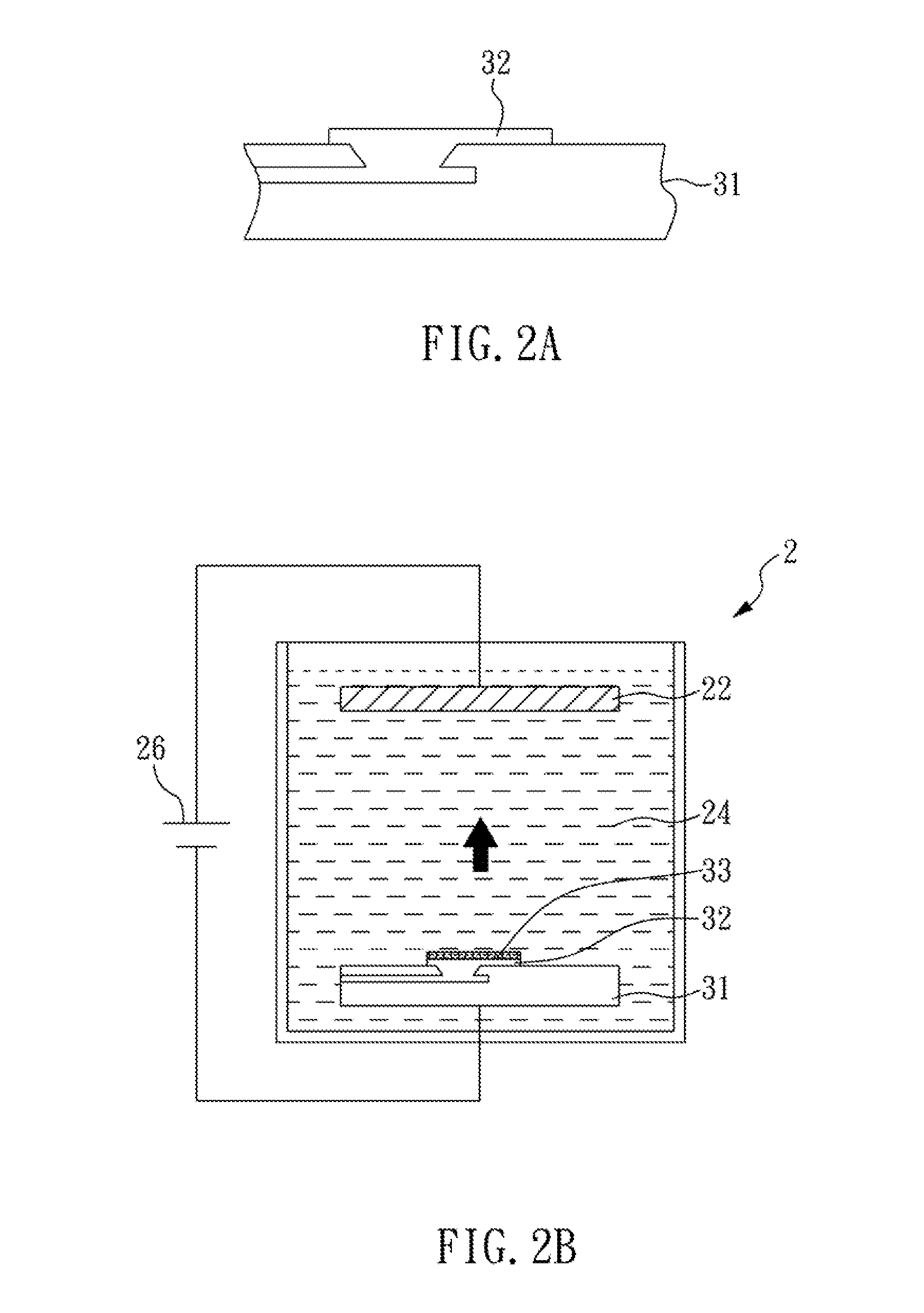
[0055]FIGS. 2A to 2D show a process for fabricating an electric connecting structure according to Embodiment 1 of the present invention. As shown in FIG. 2A, a substrate 31 is provided. In the present embodiment, the substrate 31 is a circuit board with a circuit layer 32 (which can also be used as an electrical pad). Next, as shown in FIG. 2B, the substrate 31 is placed into an electroplating device 2 to use as a cathode. The electroplating device 2 comprises an anode 22, which is immersed in an electroplating solution 24 and electrically connects to a direct current power supply source 26 (Keithley 2400 is used herein). The material used in anode 22 can be copper, phosphor bronze or inert anode material such as platinum plating titanium. The electroplating solution 24 comprises copper sulfate (copper ion concentration being 20-60 g / L), chlorine ion (concentration being 10-100 ppm), and methyl sulfonate (concentration being 80-120 g / L), and other surfactants or lattice...
embodiment ] 2
[Embodiment]2
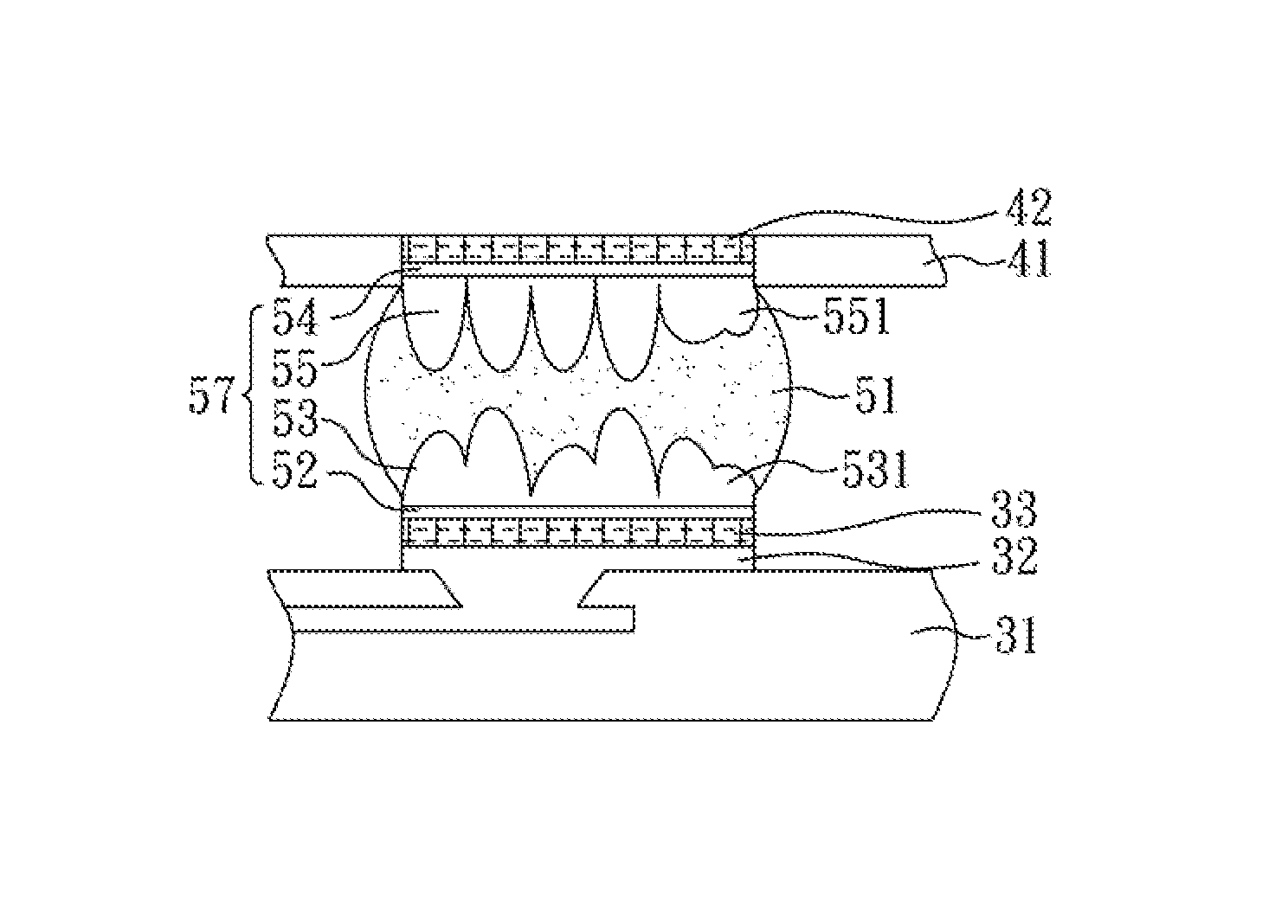
[0063]FIG. 5 is a perspective view showing an electric connecting structure of the present embodiment. The structure and the fabricating method of the electric connecting structure of the present embodiment is similar to that of Embodiment 1, except that the reflow time used in the present embodiment is longer than that used in Embodiment. The reflow time is about 5-6 min, so the size of the Cu6Sn5 grains 551, 531 is increased and the thickness of the Cu6Sn5 layer 55 is increased to about 10 μm-30 μm. In the present embodiment, the thickness of the solder 51 and the reflow time performed thereon are adjusted, so the Cu6Sn5 grains 551, 531 on the surfaces of the substrate 31 and the semiconductor 41 can be adhered to each other. In addition, the inventor confirmed that the Cu6Sn5 grains are still well oriented, even though the Cu6Sn5 grains 551, 531 are adhered to each other. The aforementioned result indicates that the method of the present invention can control the gro...
PUM
| Property | Measurement | Unit |
|---|---|---|
| thickness | aaaaa | aaaaa |
| thickness | aaaaa | aaaaa |
| temperature | aaaaa | aaaaa |
Abstract
Description
Claims
Application Information


