Insulating film, formation method thereof, semiconductor device, and manufacturing method thereof

a technology of semiconductor devices and insulating films, which is applied in the direction of transportation and packaging, coatings, layered products, etc., can solve the problems of large leakage current flowing between the source and the drain of the transistor, adversely affecting the electrical characteristics of the transistor, and ineffective suppression of oxygen vacancies, etc., to achieve excellent electrical characteristics, increase the amount of oxygen supplied by the insulating film, and improve the crystallinity of the oxide semiconductor layer

Inactive Publication Date: 2015-03-03
SEMICON ENERGY LAB CO LTD
View PDF136 Cites 5 Cited by
  • Summary
  • Abstract
  • Description
  • Claims
  • Application Information

AI Technical Summary

Benefits of technology

[0012]In a semiconductor device such as a transistor including an oxide semiconductor, when heat treatment is performed in a step after the formation of an oxide semiconductor film or when a film is formed over the oxide semiconductor film, oxygen in the oxide semiconductor film might be eliminated and oxygen vacancies might be generated owing to the influence of heat applied to the oxide semiconductor film. The oxygen vacancy in the oxide semiconductor film serves as a source of carriers and thus adversely affects electrical characteristics of the transistor. In particular, when a region where a number of oxygen vacancies are formed is placed between a source and a drain, the region serves as an unintentional path of carriers, that is, a parasitic channel, resulting in a problem of large leakage current flowing between the source and the drain of the transistor.

Problems solved by technology

The oxygen vacancy in the oxide semiconductor film serves as a source of carriers and thus adversely affects electrical characteristics of the transistor.
In particular, when a region where a number of oxygen vacancies are formed is placed between a source and a drain, the region serves as an unintentional path of carriers, that is, a parasitic channel, resulting in a problem of large leakage current flowing between the source and the drain of the transistor.
Thus, such a material is not effective for suppressing oxygen vacancies in the oxide semiconductor film.

Method used


Image

  • Insulating film, formation method thereof, semiconductor device, and manufacturing method thereof
  • Insulating film, formation method thereof, semiconductor device, and manufacturing method thereof
  • Insulating film, formation method thereof, semiconductor device, and manufacturing method thereof

Examples


embodiment 1

[0058]In this embodiment, characteristics of an insulating film of one embodiment of the present invention and a method for forming the insulating film will be described with reference to the drawings.

[Structural Example of Insulating Film]

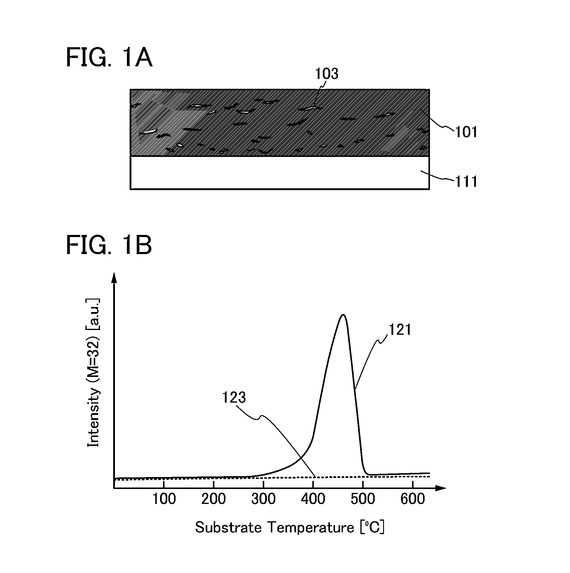
[0059]A structural example of the insulating film of one embodiment of the present invention will be described below with reference to FIGS. 1A and 1B. FIG. 1A is a schematic cross-sectional view of an insulating film 101 of one embodiment of the present invention, formed over a substrate 111.

[0060]The insulating film 101 is an oxide insulating film containing at least zirconium.

[0061]As a material of the insulating film 101, besides zirconium oxide, zirconium oxide to which yttrium oxide is added is preferably used, so that the thermal stability is increased. Such zirconium oxide to which yttrium oxide is added is also referred to as yttria-stabilized zirconia (YSZ). For example, the YSZ may contain zirconium oxide and yttrium oxide at 0.57:0.43 ...

embodiment 2

[0092]In this embodiment, a semiconductor device to which the insulating film described in Embodiment 1 as an example is applied and a method for manufacturing the semiconductor device will be described with reference to the drawings.

[0093]Note that in this embodiment, the description of the same portions as in the above embodiment is omitted or is simply given.

Structural Example 1

[0094]In this structural example, a structure of a top-gate transistor to which the insulating film of one embodiment of the present invention is applied will be described.

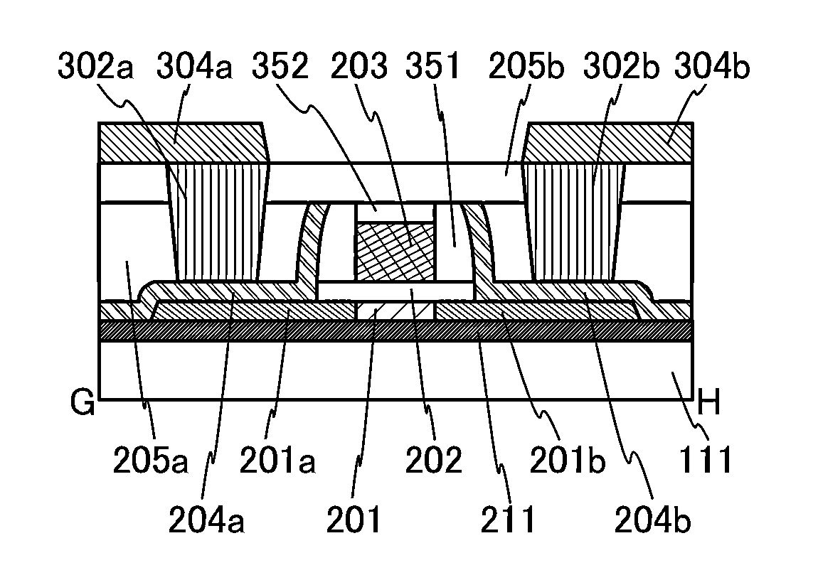
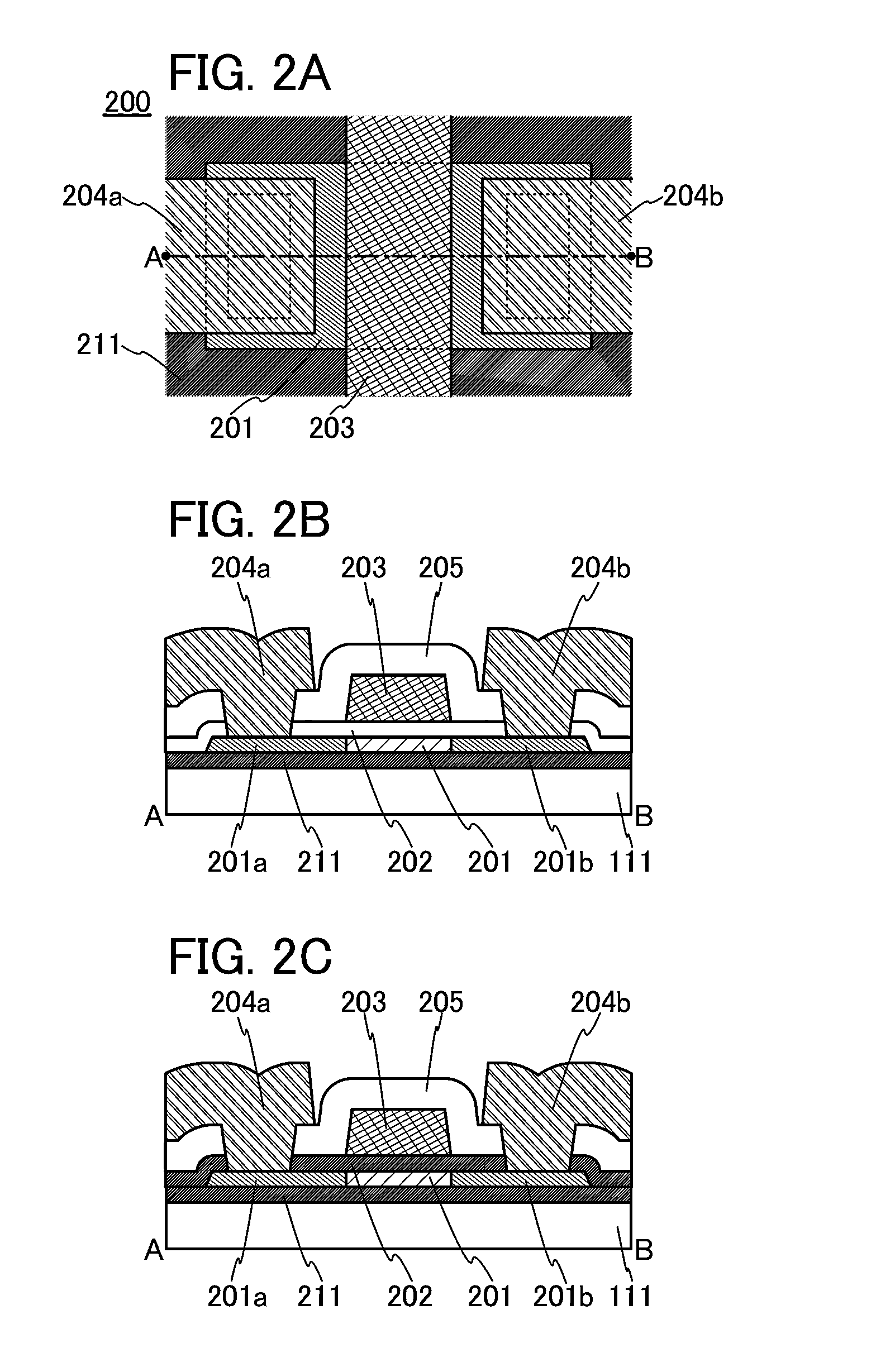
[0095]FIG. 2A is a schematic top view of a transistor 200 of one embodiment of the present invention. FIG. 2B is a schematic cross-sectional view along line A-B in FIG. 2A. Note that some components (e.g., a gate insulating layer) are not illustrated in FIG. 2A for simplicity.

[0096]The transistor 200 includes a semiconductor layer 201 including regions 201a and 201b having reduced resistance, which is in contact with the top surface of a...

process example 1

Manufacturing Process Example 1

[0122]An example of a manufacturing process of the transistor 200 described in Structural Example 1 will be described below with reference to the drawings. FIGS. 3A to 3D are schematic cross-sectional views illustrating an example of a manufacturing process of the transistor 200.

[0123]First, the substrate 111 is prepared. Although there is no particular limitation on a substrate that can be used as the substrate 111, it is necessary that the substrate have heat resistance to withstand at least a heat treatment performed later. For example, a glass substrate such as a barium borosilicate glass substrate or an aluminoborosilicate glass substrate, a ceramic substrate, a quartz substrate, a sapphire substrate, or the like can be used. Alternatively, a single crystal semiconductor substrate or a polycrystalline semiconductor substrate made of silicon or silicon carbide, a compound semiconductor substrate made of silicon germanium or the like, an SOI substra...


PUM

PropertyMeasurementUnit
temperatureaaaaaaaaaa
densityaaaaaaaaaa
temperatureaaaaaaaaaa

Abstract

An amorphous region with low density is formed in an oxide insulating film containing zirconium. The amount of oxygen released from such an oxide insulating film containing zirconium by heating is large and a temperature at which oxygen is released is higher in the oxide insulating film than in a conventional oxide film (e.g., a silicon oxide film). When the insulating film is formed using a sputtering target containing zirconium in an oxygen atmosphere, the temperature of a surface on which the insulating film is formed may be controlled to be lower than a temperature at which a film to be formed starts to crystallize.

Description

BACKGROUND OF THE INVENTION[0001]1. Field of the Invention[0002]The present invention relates to an insulating film and a method for forming the insulating film. The present invention also relates to a semiconductor device and a method for manufacturing the semiconductor device.[0003]In this specification and the like, a “semiconductor device” generally means any device which can function by utilizing semiconductor characteristics, and an electro-optical device, a semiconductor circuit, and an electronic device are all semiconductor devices.[0004]2. Description of the Related Art[0005]A technique by which a thin film transistor is formed using a semiconductor thin film formed over an insulating surface has attracted attention. The transistor is applied to a wide range of electronic devices such as an integrated circuit (IC) and an image display device (display device). As a material of a semiconductor thin film applicable to the transistor, for example, a silicon based semiconductor...

Claims


Application Information

Patent Timeline
Patent Type & Authority Patents(United States)
IPC IPC(8): H01L21/00H01L21/02H01L21/36H01L29/66H01L29/786
CPCH01L29/7869H01L21/36H01L29/66742H01L29/78603H01L21/02189H01L21/02194H01L21/02266H01L29/66969Y10T428/24628
Inventor TANAKA, TETSUHIROTAKAHASHI, ERIKAIMOTO, YUKISATO, YUHEI
Owner SEMICON ENERGY LAB CO LTD
Why Eureka
Try Eureka