

Organic compound and organic electroluminescent device using the same
a technology of organic compound and electroluminescent device, which is applied in the field of organic compound and organic electroluminescent, can solve the problems of power consumption, unsatisfactory half-life of organic compound used for organic multi-layer, and emitted colour, and achieve the effect of shortening half-life and reducing efficiency
- Summary
- Abstract
- Description
- Claims
- Application Information
AI Technical Summary
Benefits of technology
Problems solved by technology
Method used
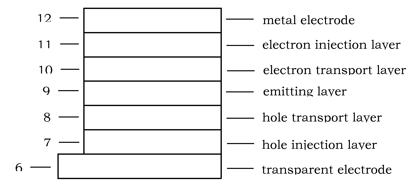
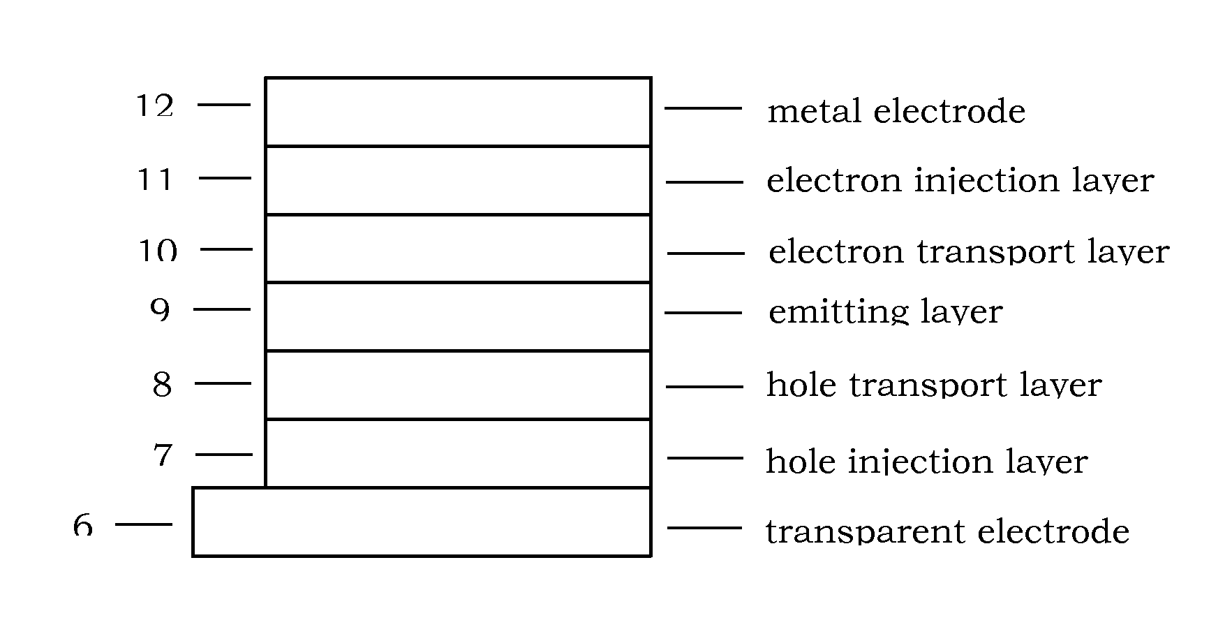
Image

Examples
example 1
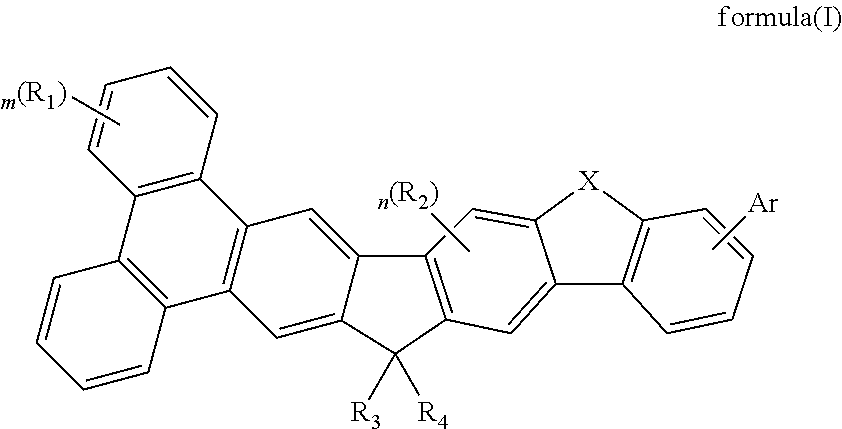
Synthesis of Compound II-2
Synthesis of 1,4-diphenyl-2,5-dimethylbenzene
[0029]
[0030]A mixture of 52.8 g (200 mmol) of 1,4-dibromo-2,5-Dimethyl benzene, 53.6 g (440 mmol) of phenylboronic acid, 2.3 g (2 mmol) of tetrakis(triphenylphosphine)palladium, 400 ml of 2M Na2CO3, 400 ml of EtOH and 800 ml toluene was degassed and placed under nitrogen, and then heated at 90° C. for 6 hours. After the reaction finish, the mixture was allowed to cool to room temperature. The organic layer was extracted with ethyl acetate and water, dried with anhydrous magnesium sulfate, the solvent was removed and the residue was purified by column chromatography on silica (hexane-dichloromethane) to give product 43.4 g (168 mmol, 84%) as a white solid.
Synthesis of 2,5-diphenylterephthalicacid
[0031]
[0032]To a solution of 1,4-diphenyl-2,5-dimethylbenzene 43.4 g (168 mmol) in pyridine (450 ml) was added a hot KMnO4 solution (239 g in 700 ml H2O) over 1 h under reflux and the reaction was stirred at 130° C. for 12...
example 2
Synthesis of Compound II-10
[0049]
[0050]A mixture of 2.1 g (10 mmol) of 2-bromonaphthalene, 7 g (12 mmol) of Intermediate II, 0.12 g (0.1 mmol) of tetrakis(triphenylphosphine)palladium, 10 ml of 2M Na2CO3, 30 ml of EtOH and 100 ml toluene was degassed and placed under nitrogen, and then heated at 90° C. for 12 h. After finishing the reaction, the mixture was allowed to cool to room temperature. Than 500 ml MeOH was added, while stirring and the precipitated product was filtered off with suction. To give 4 g (yield 69%) of yellow product which was recrystallized from toluene. MS (m / z, FAB+): 586.4; 1H NMR (CDCl3, 400 MHz): chemical shift (ppm) 9.11 (s, 1H), 8.76˜8.68 (m, 2H), 8.61 (s, 1H), 8.35 (d, J=8.0 Hz, 1H), 8.08˜7.94 (m, 2H), 7.86˜7.61 (m, 5H), 7.55˜7.42 (m, 6H), 7.31˜7.26 (m, 2H), 7.13 (s, 1H), 7.04 (s, 1H), 1.82 (s, 6H), 1.80 (s, 6H).
example 3
Synthesis of compound II-12
[0051]
[0052]A mixture of 2.6 g (10 mmol) of 9-bromoanthracene, 7 g (12 mmol) of Intermediate II, 0.12 g (0.1 mmol) of tetrakis(triphenylphosphine)palladium, 10 ml of 2M Na2CO3, 30 ml of EtOH and 100 ml toluene was degassed and placed under nitrogen, and then heated at 90° C. for 12 h. After finishing the reaction, the mixture was allowed to cool to room temperature. Than 500 ml MeOH was added, while stirring and the precipitated product was filtered off with suction. To give 2 g (yield 32%) of yellow product which was recrystallized from toluene. MS (m / z, FAB+): 636.9; 1H NMR (CDCl3, 400 MHz): chemical shift (ppm) 9.13 (s, 1H), 8.78˜8.70 (m, 3H), 8.68 (s, 1H), 8.42 (d, J=8.0 Hz, 1H), 8.21˜7.94 (m, 3H), 7.83 (d, J=8.0 Hz, 2H), 7.79˜7.57 (m, 7H), 7.43˜7.36 (m, 2H), 7.31˜7.26 (m, 2H), 7.17 (s, 1H), 7.06 (s, 1H), 1.82 (s, 6H), 1.80 (s, 6H).
PUM
| Property | Measurement | Unit |
|---|---|---|
| temperature | aaaaa | aaaaa |
| temperature | aaaaa | aaaaa |
| temperature | aaaaa | aaaaa |
Abstract
Description
Claims
Application Information